There’s a lot of research activity on new electronic and optoelectronic devices based on vertical heterostructures of 2D materials, because there are many materials available and even more combinations.
To accelerate materials selection and to support experiments it is important to be able to simulate their behaviour in a way that is quantitatively predictive and computationally doable.
Kudos to Giuseppe Lovarelli, Gaetano Calogero, and Gianluca Fiori.
In the paper, we propose a computationally effective and physically sound method to model electron transport in 2D van der Waals heterostructures, based on a multiscale approach and quasiatomistic Hamiltonians.
This is something important for us in the Quantum Engineering for Machine Learning project, where we use devices based on lateral and vertical heterostructures of 2D materials to demonstrate analog neural networks. For example, we use the method for computing the leakage current through the vertical stack of an analog non volatile memory.
Good step for us towards a fully analog neural network chip, using standard CMOS technology, while in parallel we explore the possibility of building them with 2D materials in the QUEFORMAL project.
Here, we experimentally demonstrated the most important computational block of a deep neural network, the vector matrix multiplier, in standard CMOS technology with a high-density array of analog non-volatile memories, forcing the technology “out of its comfort zone” (and out of qualification).
Essentially, we used a transistor as a two-terminal analog non-volatile memory, leaving the gate floating. We were able to program and erase the memory with high accuracy via a program and verify scheme using a sequence of short pulses of increasing amplitude.
The circuit multiplies an array of input quantities (encoded in the time duration of a pulse) times a matrix of trained parameters (“weights”) encoded in the current of memories under bias. The output is converted in an array of voltages by an array of transresistive amplifiers.
The effective number of bits of the analog operation is 6, which is good enough to obtain high classification accuracy and correspond to a record energy efficiency of 100 Teraoperations per Joule.
A fully analog neural network will be able to bring cognitive capability on very small battery operated devices, such as drones, watches, glasses, industrial sensors, and so on.
The basic premise of the quantum reconstruction game is summed up by the joke about the driver who, lost in rural Ireland, asks a passer-by how to get to Dublin. “I wouldn’t start from here,” comes the reply.
Where, in quantum mechanics, is “here”? The theory arose out of attempts to understand how atoms and molecules interact with light and other radiation, phenomena that classical physics couldn’t explain. Quantum theory was empirically motivated, and its rules were simply ones that seemed to fit what was observed. It uses mathematical formulas that, while tried and trusted, were essentially pulled out of a hat by the pioneers of the theory in the early 20th century.
Quantum mechanics is at the basis of the operation of solid-state electronics and optoelectronics, and therefore enables the whole ICT and Internet world.
However, it is still introduced to students as a new science, a revolution with respect to “classical” science, and as something that is basically strange and unintuitive. This is because the historical view of the birth of quantum mechanics is still dominant, after all these years. So all new attempts at rebuilding the foundations of quantum physics are welcome (and I admit I still very much like David Bohm’s view).
Questa è una breve intervista nella trasmissione Community del canale Rai Italia, dedicato agli italiani all’estero. Mi piace sempre cercare di comunicare il senso della ricerca che facciamo al pubblico generale (che indirettamente paga il conto).
La cosa difficile per me è evitare affermazioni senzazionali e allo stesso tempo non essere troppo noioso, essere accurato ma non apparire pedante, far capire che è normale che solo una piccola frazione della ricerca di frontiera porti a una innovazione tecnologica nel mondo reale.
Sopratutto, narrazione a parte, nell’evoluzione della scienza e della tecnologia ciascun gruppo di ricerca in realtà dà un piccolo contributo a una storia molto più grande, a cui partecipano decine di migliaia di persone. Lavoriamo da alcuni anni sulla nanoelettronica con materiali bidimensionali e ancora lavoreremo, esaltati dalle grandi potenzialità e alle prese con i numerosi problemi.
The Nanohub has recently posted this a video of a presentation I gave last September during the International Workshop on Computational Electronics, at Purdue University in West Lafayette, Indiana. It is some of our most recent work on electronics based on two-dimensional materials.
I really like the software platform, with video and audio, slides, and the table of contents in the same page. There’s a lot of great educational and academic content on the Nanohub, for the curious and the professional.
Click here to see the presentation in html format (video and syncronized high definition slides), or one the youtube video below.
This is the transcript of a talk I gave in Siena on 26 June 2015, for the annual meeting of the Italian association of scholars and researchers in Electronics (“Gruppo Italiano Elettronica”).
Semiconductor electronics was shaped in a form very close to the present one between the 30s and the 60s, as a distinct discipline with respect to solid-state physics and vacuum-tube electronics. During those developments it became clear that some electrical engineers had to be trained as scientists, and the first PhD program for engineers was started at MIT in 1952 after the initiative of Gordon Brown, then Head of the Department of Electrical Engineering.
Already in 1932, in a paper on Zeitschift fur Physik on the theory of metal-semiconductor diodes, we see a illustration of the principle of operation using the now common band-edge profiles.
Figure from Zur Theorie der Detektorwirkung”, Zeitschrift fur Physik, 1932, 75, 434
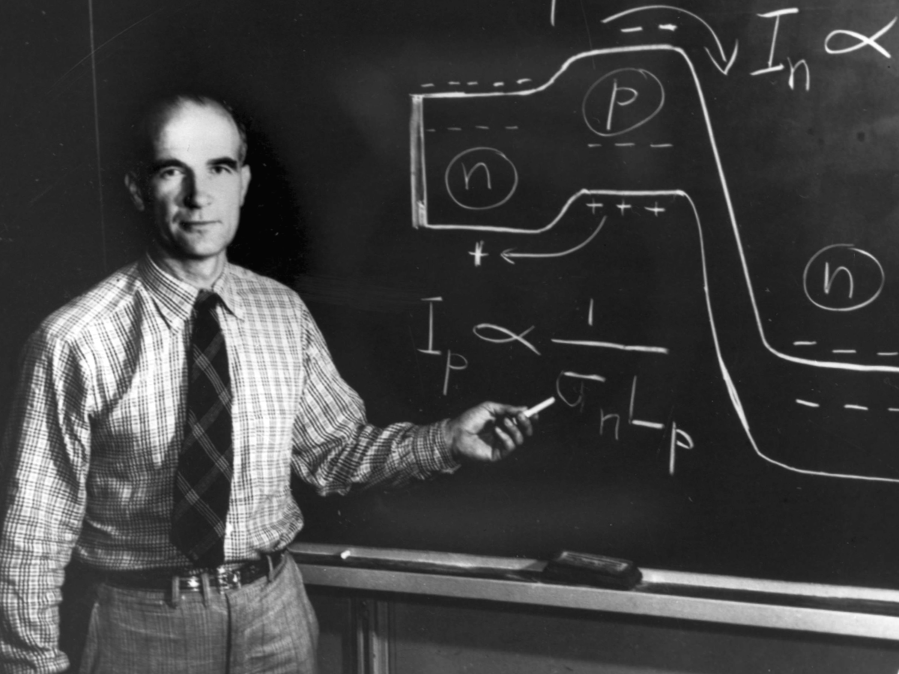
And this is a photo of Shockley from 1950, where we can clearly see the band-edge profiles of a bipolar junction transistor. This graphic way of describing the operation of semiconductor devices became common in the 30s. Basically, if you take a modern textbook or some modern papers, you find a very similar way of describing transistor operation.
William Shockley, photo courtesy of Alcatel-Lucent USA Inc.
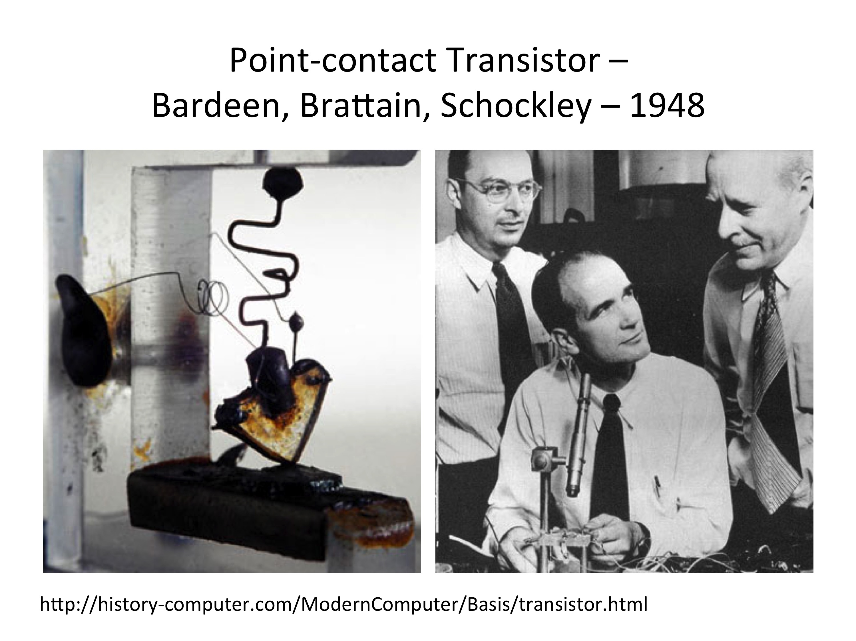
Why semiconductor electronics has be so successful for such a long time? Let’s look at what happened. Bardeen, Brattain and Shockley invented the first transistor in 1948. They actually were trying to obtain a field-effect transistor, but it worked out differently, and they obtained the point-contact transistors.
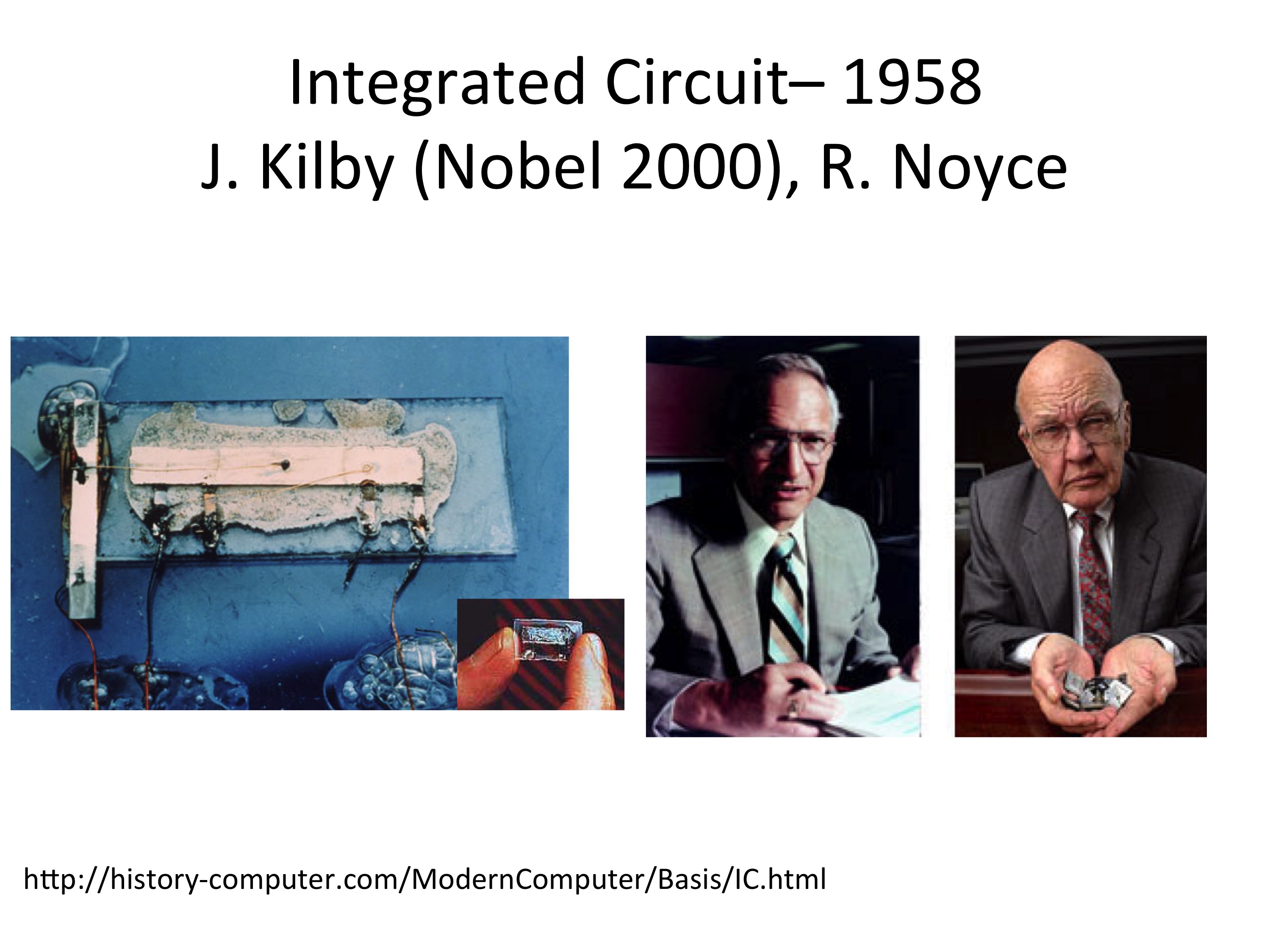
The first transistor made of germanium one, then silicon became the material of choice, right after the invention of the integrated circuit by Kilby and Noyce. Silicon oxide was a very good dielectric and could be grown on silicon.
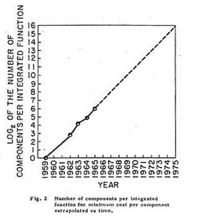
The integrated circuit allow the industry to double every 1–2 years the number of transistors on a single chip. And it is still working now, at a few billion transistors per chip. This exponential behaviour came to be known as Moore’s law, after a prediction that Gordon Moore made in 1965, with only few data points, exactly 50 years ago.
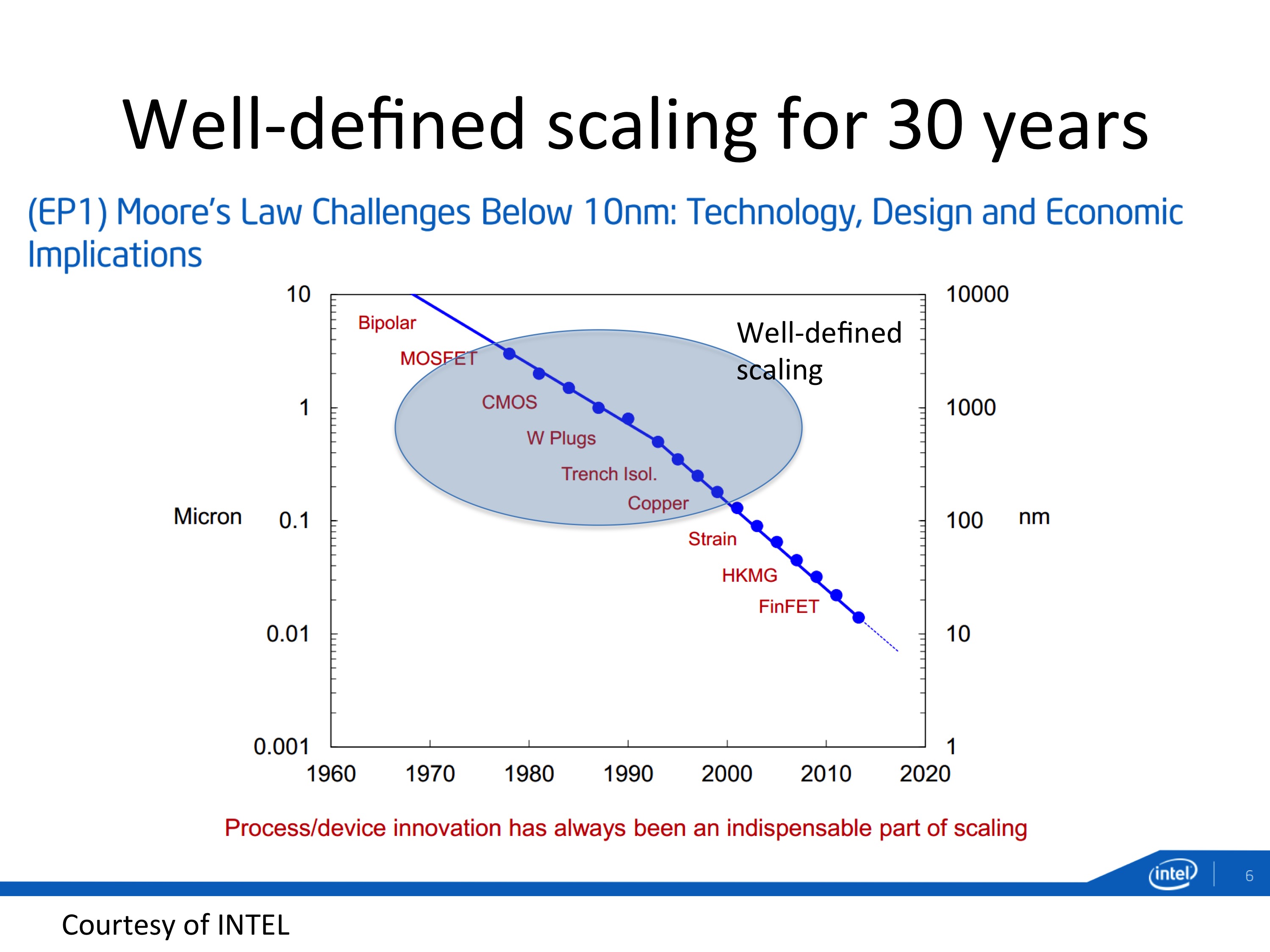
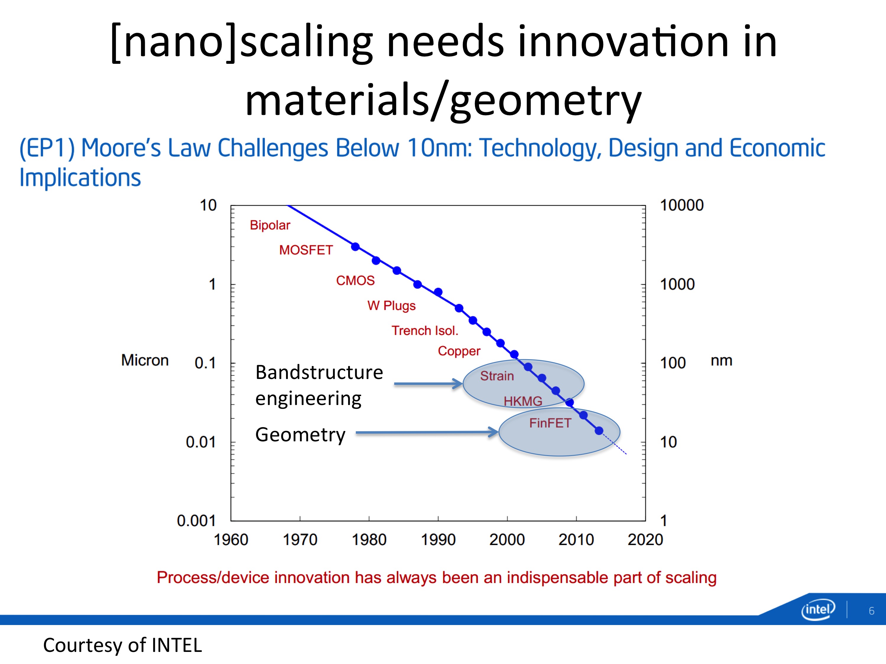
Actually, after moving from Bipolar devices to NMOS and to CMOS, the track to scaling was well defined. I do not want to discard the huge investment in technology that was required, but from the device point of view, little changed in terms of materials and geometries except for scaling.
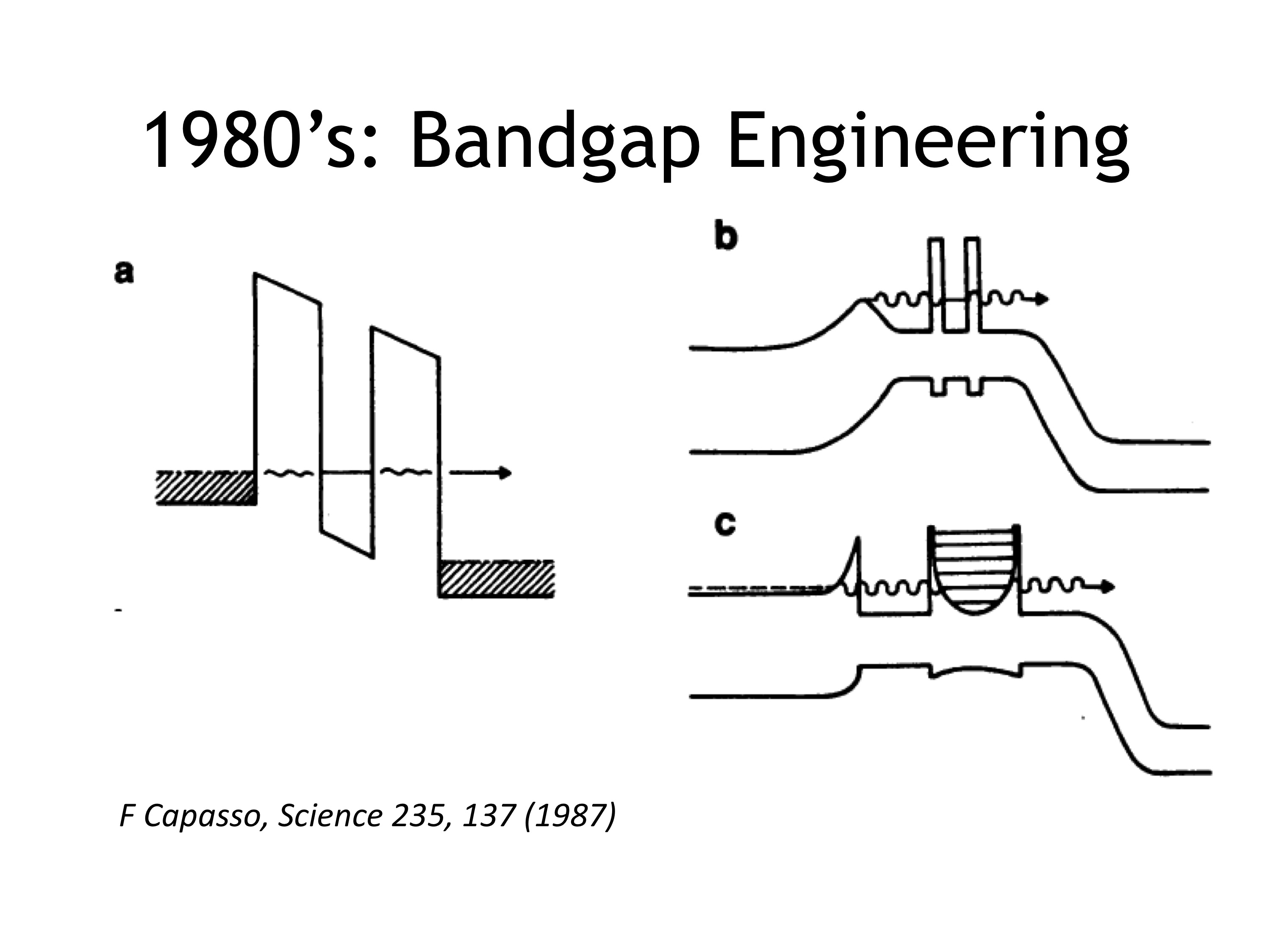
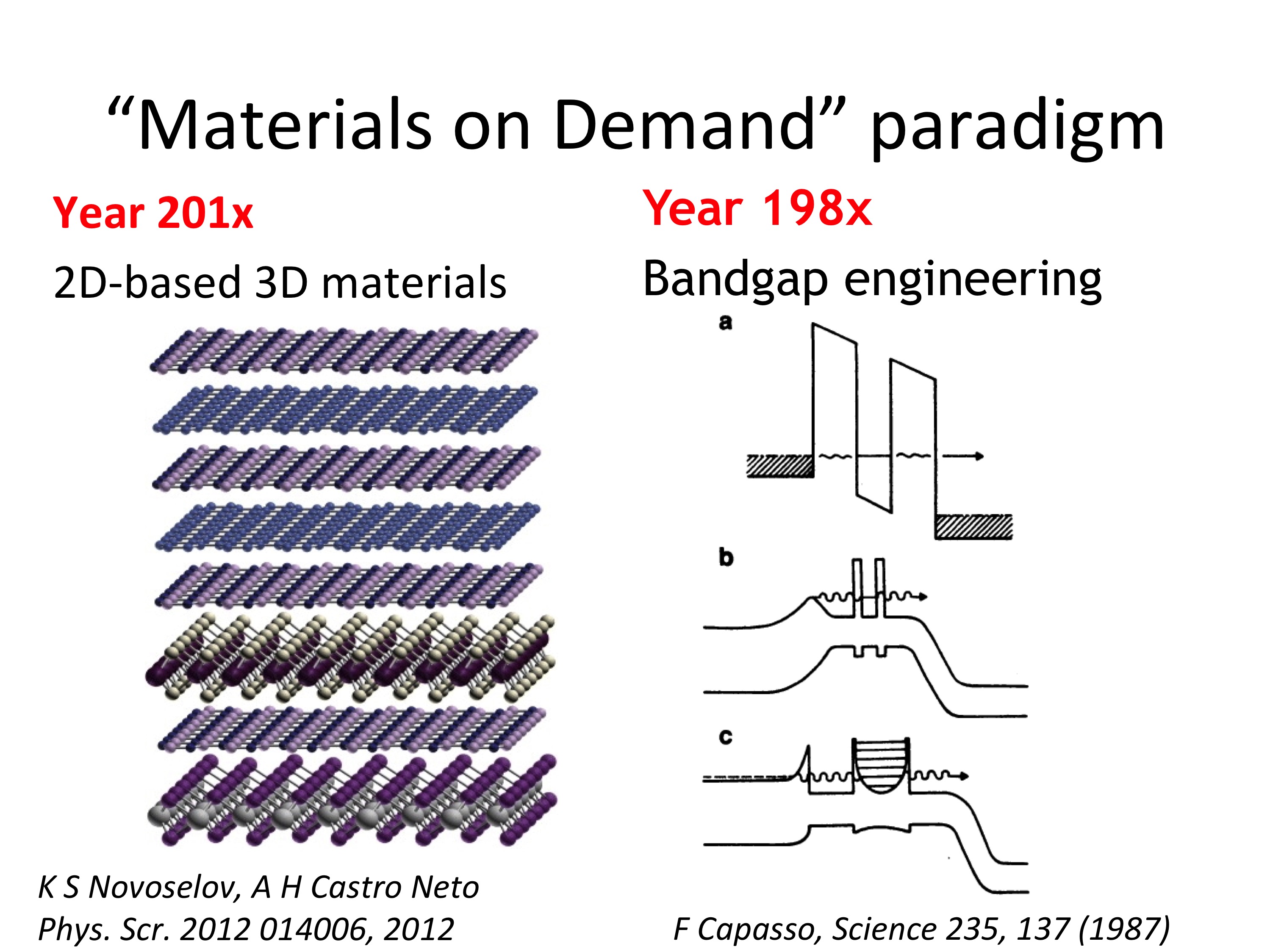
But in the 80s already someone started to see that scaling was becoming harder, and that therefore some intrinsic limitations were present. Some alternatives were proposed: one very interesting at the time was the so-called bandgap engineering, which was proposed among others by Federico Capasso, then at Bell Labs. The core of the proposal was to exploit the newly available growth techniques to fabricated heterostructures and superlattices in order to adjust the bandstructures to optimize existing devices or create new device concepts.Actually it did not go this way and it never made into the mainstream in this form. The semiconductor industry found new ways to proceed with the scaling down, leaving the device structure unaltered.
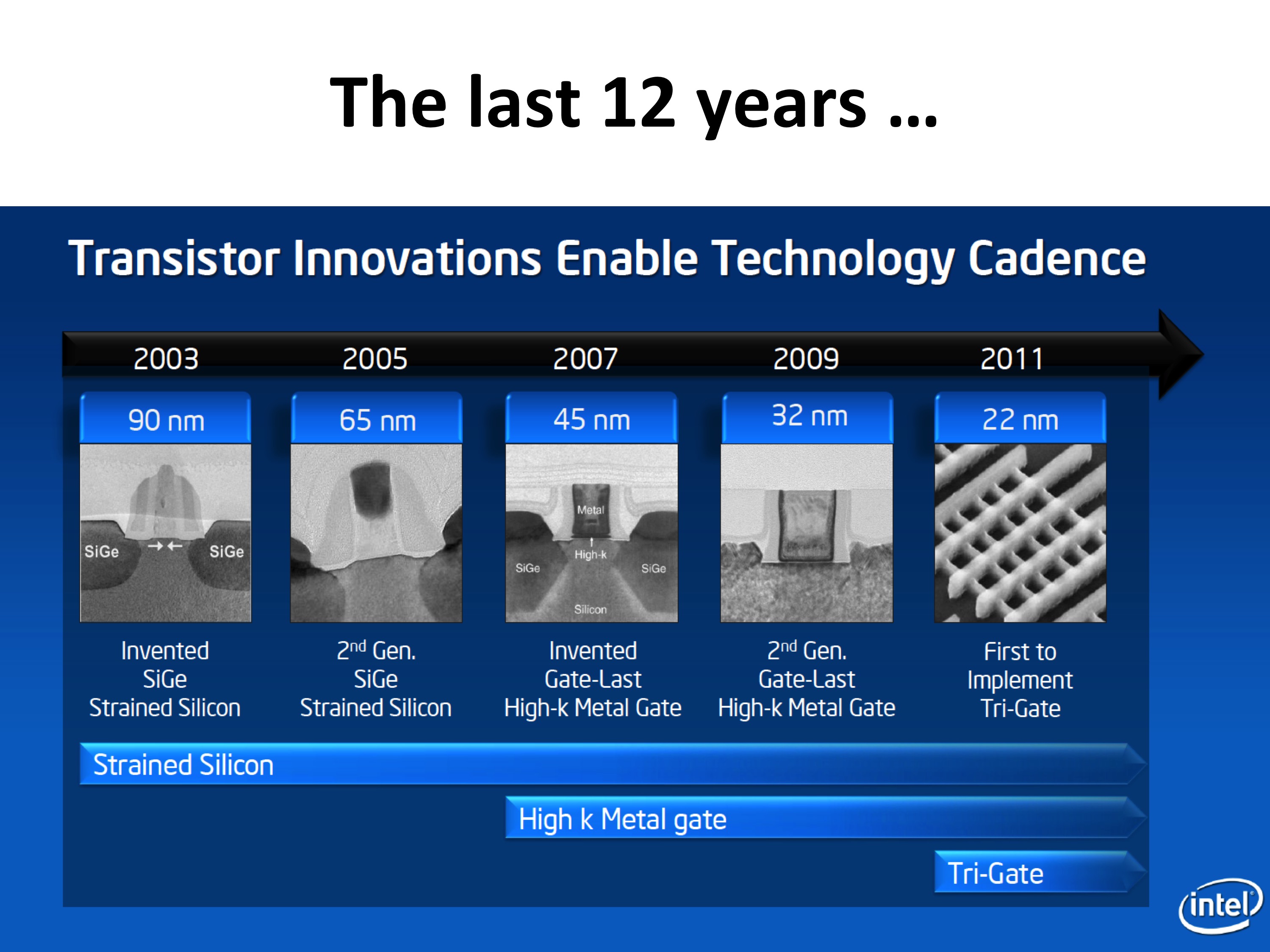
But then, something happened 12 years ago. Scaling continued, but strong innovations had to be introduced in terms of materials and structure.
First, in 2003, strained silicon. We stretch the silicon crystal to modify the bandstructure, to adjust the energy of conduction band minima and valence band maxima, and to modify the effective mass, in order to boost mobility. Tensile strain is needed for PMOS, compressive strain for NMOS. You can see, this is essentially a type of bandstructure engineering, which actually became mainstream, in a way different from what initially proposed.
Photo courtesy of Intel
Then in 2007, High-K metal gate process, another type of bandgap engineering. A gate stack with insulator with high dielectric constant and smaller gap, that would allow to use a thicker layer to suppress gate leakage current while maintaining good electrostatic control on the channel.
Finally, in 2011, the trigate process, i.e. no more planar transistors but a three dimensional device, to improve the electrostatic control of the channel.
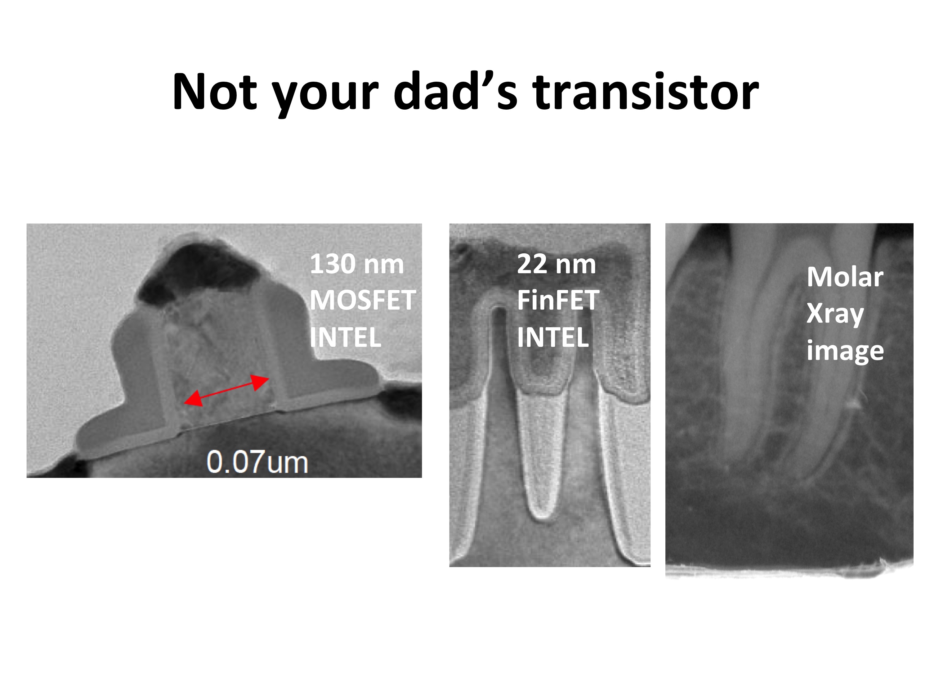
In the end we really do not recognize a transistor anymore. What’s this?
Image courtesy of Intel
You see, the image of a 22 nm transistor is closer to a molar than to a 130 nm transistor. It is definitely not your dad’s transistor.
What should we expect now?
Simply, more of the same:
moreinnovation in materials, for example III-V semiconductors, Germanium, or other 2D materials for the transistor channel
more innovation in structures, for example the use of 3D structures, which is now a reality in non-volatile memories.
more physical mechanisms, adding to transport and electrostatics also mechanics, microfluidics, optics, magnetics, piezo, thermoelectrics. For example microelectromechanical systems are already a 12 B$ global business.
Now it should be clear what is The New Semiconductor Electronics.
We had a semiconductor electronics with few materials, mainly the silicon-silicon oxide system, planar devices, and only electronics on a silicon chip.
The New Semiconductor Electronics uses a wealth of materials, geometries, and much more physical mechanisms on a silicon platform
Of course it is a huge intellectual adventure, because we need to change skin a bit, and to learn lots of new things.
Are we ready for this?
I don’t know. In the 60s, when Semiconductor Electronics was established as a distinct discipline, the Semiconductor Electronics Education Committee was established to prepare a set of six paperback textbooks to teach the subject in an adequate way.
I am trying to buy all those books from abebooks. If you read them you would notice that they are very similar to the books we use today, 50 years later.
Too similar.
We need some effort in renewing academic education and research in the field of semiconductor electronics.
Things have not only become more complicate in the new semiconductor electronics. Indeed, other things are simpler at the nanoscale!
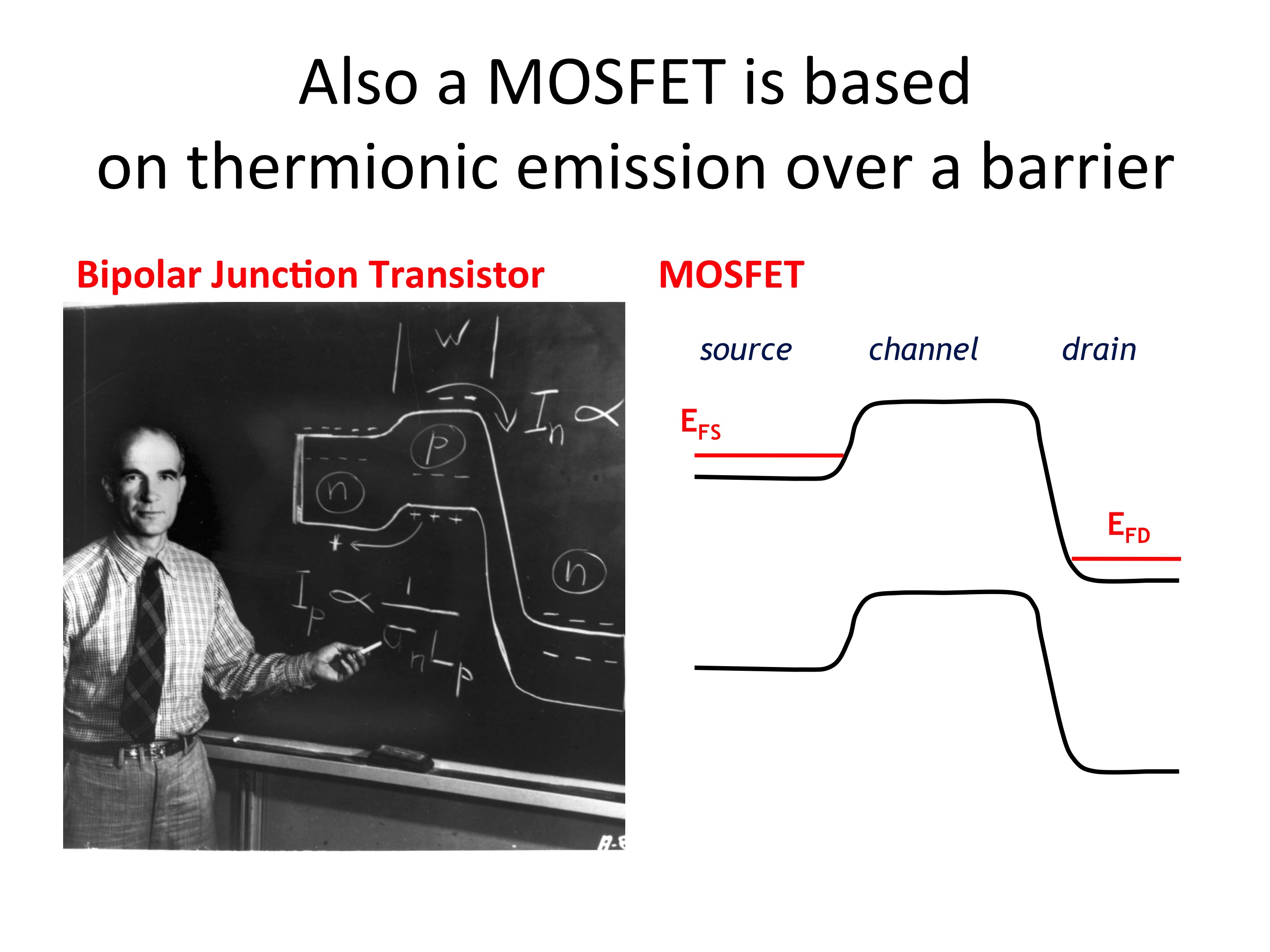
For example, in traditional semiconductor electronics we look at bipolar junction transistors and at field-emission transistors as different devices, the former dominated by diffusion currents, and the second by drift currents.
However, for small channel length, if we look at the band edge profiles of the two devices, as shown in the figure below, we clearly see that they are identical, and that both devices are described by the same physical mechanism: thermionic emission over a tunable barrier.
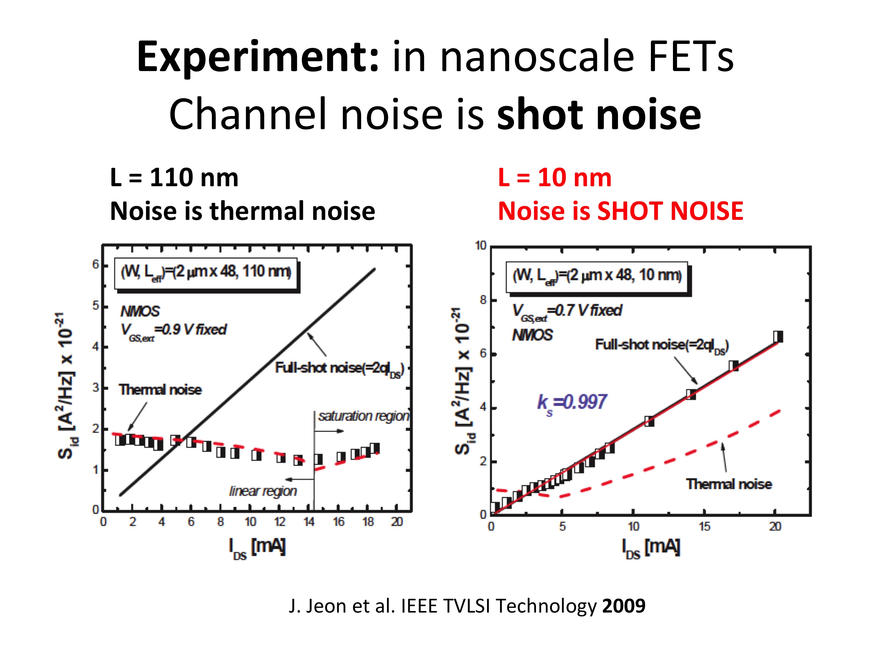
As far as noise is concerned, we learn from traditional device electronics book that shot noise describes the current noise in a bipolar transistor, and that “corrected” thermal noise describes current noise in a field-effect transistor. However, it is well known that as channel length is decreases the latter correction becomes larger and larger, in order to enable the model to reproduce reality.
The fact is that in nanoscale FETs the operating mechanism is similar as that of a bipolar transistor, and therefore “suppressed” shot noise is the proper noise mechanism also describing an FET. The “suppression” is due to the proximity of the gate contact.
This concept has been clearly expressed more than 10 years ago, and finally in recent years it has been demonstrated in experiments on 10-nm long FETs.
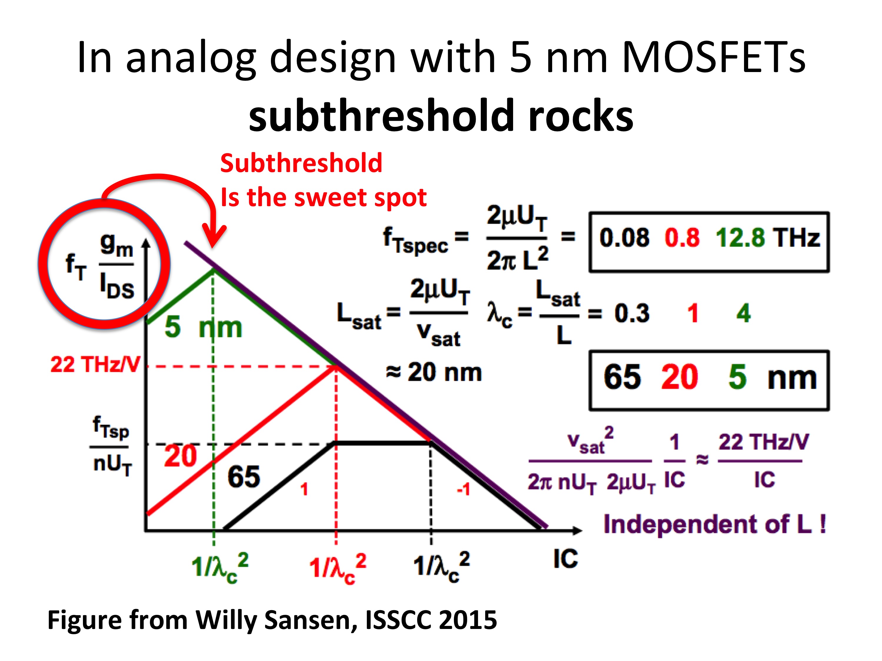
As a third example, let me show this figure from Willy Sansen’s keynote at ISSCC in 2015. For analog circuit design in aggressively scaled down CMOS processes, below 20 nm: subthreshold operation provides the best figures of merit in terms of performance at power parity (the corresponding figure of merit is the cutoff frequency times the transconductance divided by the bias current).
This is very interesting, because in traditional undergraduate education the subthreshold operation of field-effect transistor is often not considered. In sub threshold operation, currents depend exponentially on bias voltages, as in bipolar transistors.
I would like now to give some examples of how we address the themes of the new semiconductor electronincs.
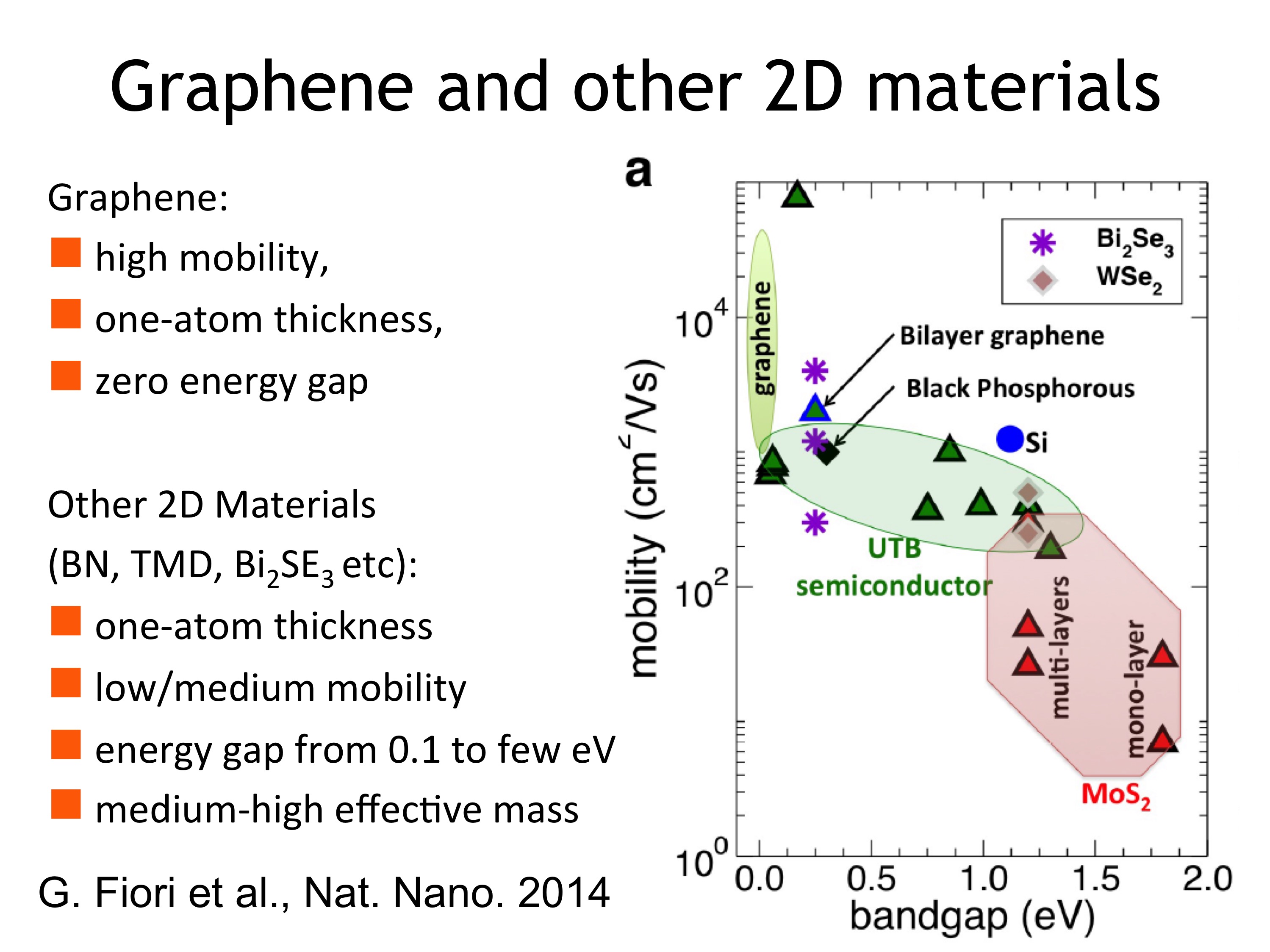
In the last decade, two dimensional materials have attracted incredible interest for applications in electronics. It all started when the electrical properties of graphene where discovered and characterized in 2004 in Manchester. Graphene is just one-atom thick, therefore is an ideal two-dimensional material, and can have a very high mobility at room temperature, close to 10,000 cm2/Vs when deposited on a substrate. However, it also have a zero energy gap, which represents a severe obstacle to its use in electronics.
After graphene, other two-dimensional materials have received enormous attention: among them boron nitride, the family of transition metal dichalcogenides, bismuth selenide and bismuth telluride, and others.
They are also very thin, generally have a medium-to-low mobility and have an energy gap from 0.1 eV to 5 eV, with the usual tradeoff between mobility and energy gap.
If we look at performance figures, such as the delay time and the dynamic power indicator, they are in the optimistic case in line with the evolution of the International Tecnology Roadmap for Semiconductor, since device modeling on defect less device structures predict comparable performance to the expectations at the end of roadmap horizon (2016).
In 2012, a “Materials on demand” Paradigm has been proposed, i.e., the possibility of obtaining 3D materials with taylored properties by stacking several layers of 2D materials coupled by Var der Waals forces.
You can probably recognize the similarity with the paradigm of “Bandgap Engineering” of the 80s that I have shown before. Of course, things are not identical: in the 80s they were considering III-V heterostructures, consisting of layers with a thickness of few nanometers, almost lattice-matched; in this case we are dealing with single atom layers, often with completely different lattice, and we are playing with a larger number of atomic species. Of course, history does not exactly repeat itself, but it rhymes?—?as Mark Twain famously said.
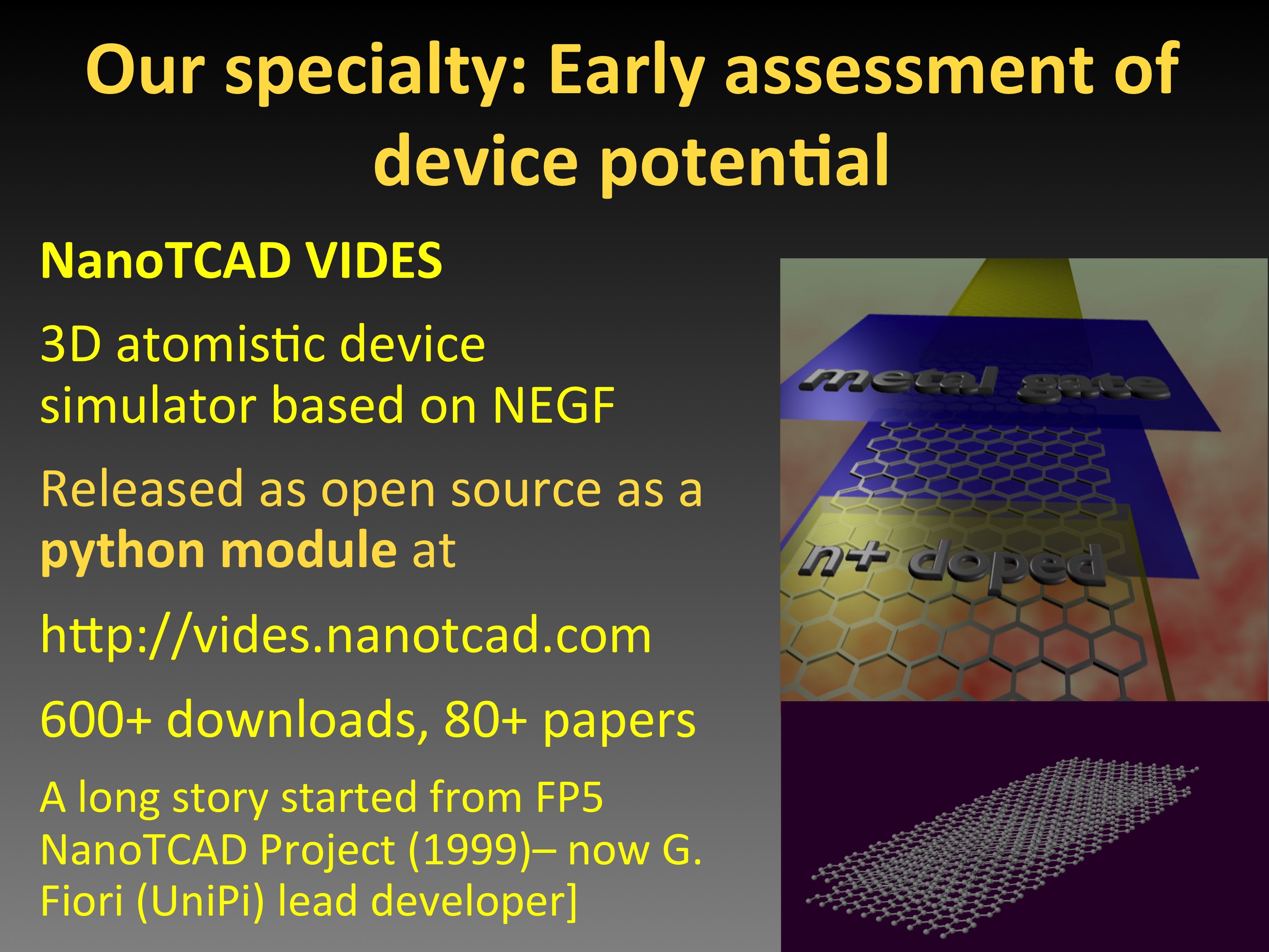
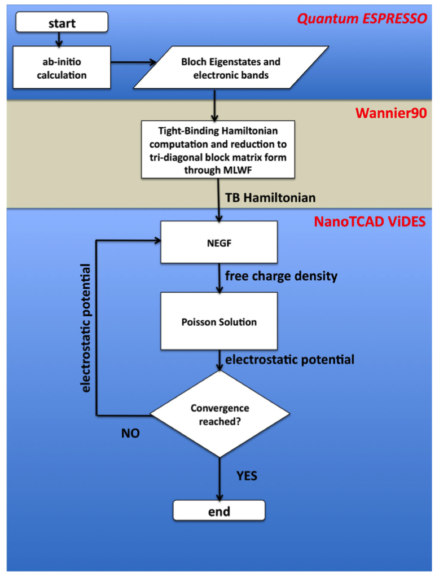
Let me say how we address these problems. Our specialty is the early assessment of device potential via modelling. In order to do that, we use our in house simulation tool, Nanotcad Vides, that now has 15 years of development. It started with a European project that I coordinated in the 5th Framework Programme from 2000 to 2003, and now has atomistic simulation capabilities of 3D devices coupling transport and electrostatics. Now the lead developer is my colleague Gianluca Fiori, we have made freely available the source code and full documentation, to let everybody use it. As of today, a few groups are using this code, also independently of us. We maintain a known list of publications using the code.
With the code we can compute transport properties of silicon and carbon based devices, using non-equilibrium Green’s functions with a tight-binding Hamiltonian, or an effective mass approach. To put it simply, we build the device or key building blocks atom by atom, and then simulate the operation of a complete device.
Our approach is to use our modeling tools, other tools, and analytical modeling to evaluate the feasibility and the possible performance of a device structure (assuming that fabrication problems will be solved). Here a mix of physicist and engineer attitude is really important. We look at new effects for opportunities, we are optimistic but skeptic, and we benchmark with existing technology and its foreseeable evolution, as for example predicted by the International Technology Roadmap for Semiconductors.
Essentially, we use a “Via Negativa” approach: we try to rapidly filter out device structures and operating principle that are not promising, and save the very few promising ones for further investigation.
Via negativa: “This won’t work. This neither. Try instead this.”
In the modern scientific PR-conscious world where hype is the norm, saying that some things do not work is not the easy way to become popular.
I need to add few more words on our methodology. We need to consider many different materials, and of some of them we have very limited information. In addition, the materials properties are affected by the by the peculiar heterostructure we choose. We then need a way to compute material properties and to use those results in the device simulations.
This requires a specific multiscale simulation procedure because ab initio quantum chemisty tools (DFT) for the calculation of material properties are very demanding from the computational point of view.
For this reason, we have recently defined this multiscale methodology according to which we use an open source DFT tool (e.g., Quantum Espresso) to make ab initio calculations, in order to compute materials properties. Once we have a good single particle Hamiltonian, we derive a TB Hamiltonian, using Wannier90 to project the Hamiltonian on a basis of localized Wannier functions. Finally, we can perform NEGF calculations with our in-house code.
In the rest of this talk, I just want to use my time to show you a device that after our via negativa test is still promising for application, to come close to an end in a positive note.
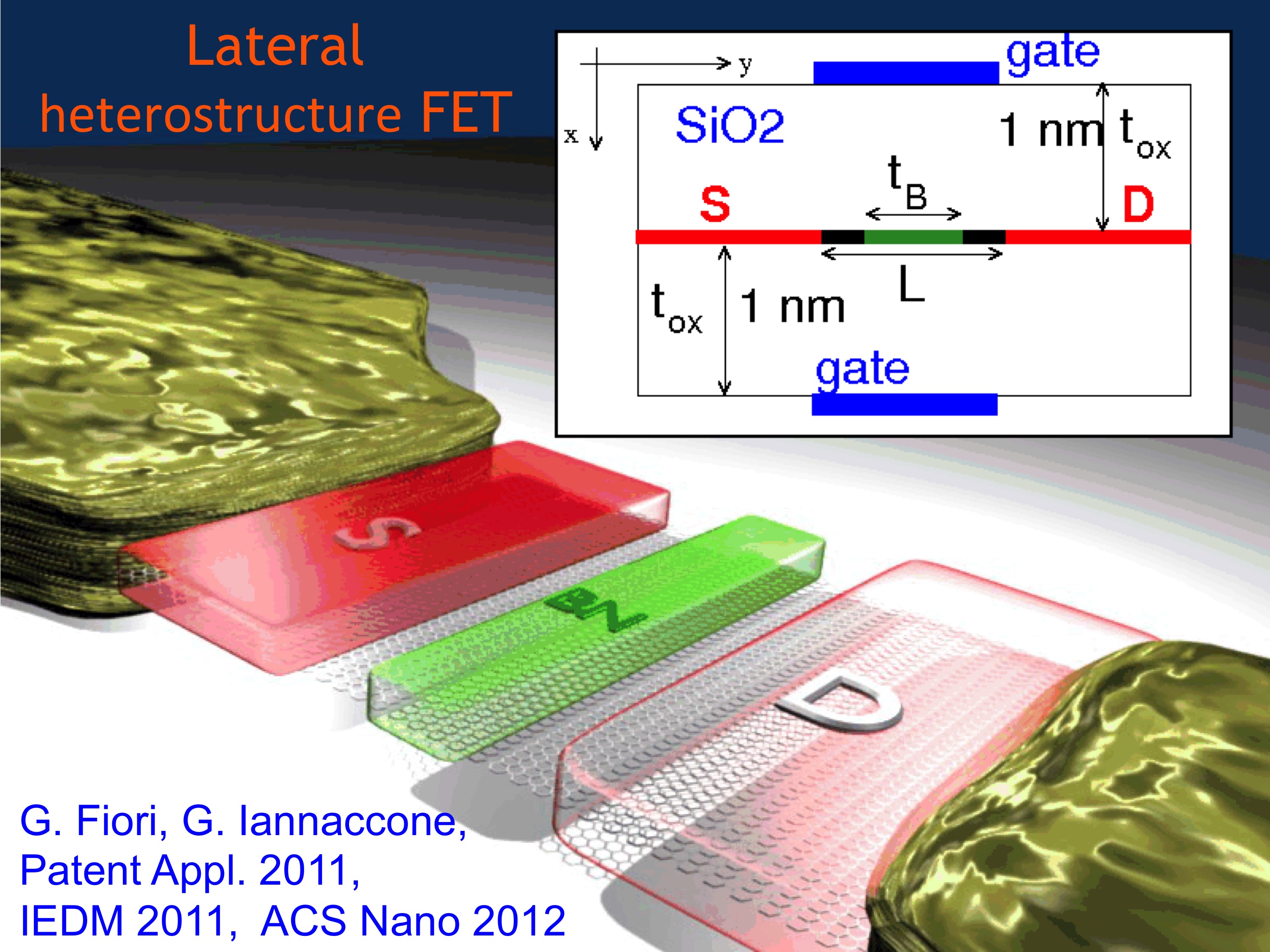
The lateral heterostructure field-effect transistor is a transistor structure we proposed in 2011. The channel consists of a lateral heterostructure, where we have on the same single sheet regions of graphene and regions of another 2D material with comparable lattice. In our case, the part of the channel under the gate is made of a large gap material, such as boron nitride, because it has to stop the current in the off state, and outer regions of source and drain are made with graphene.
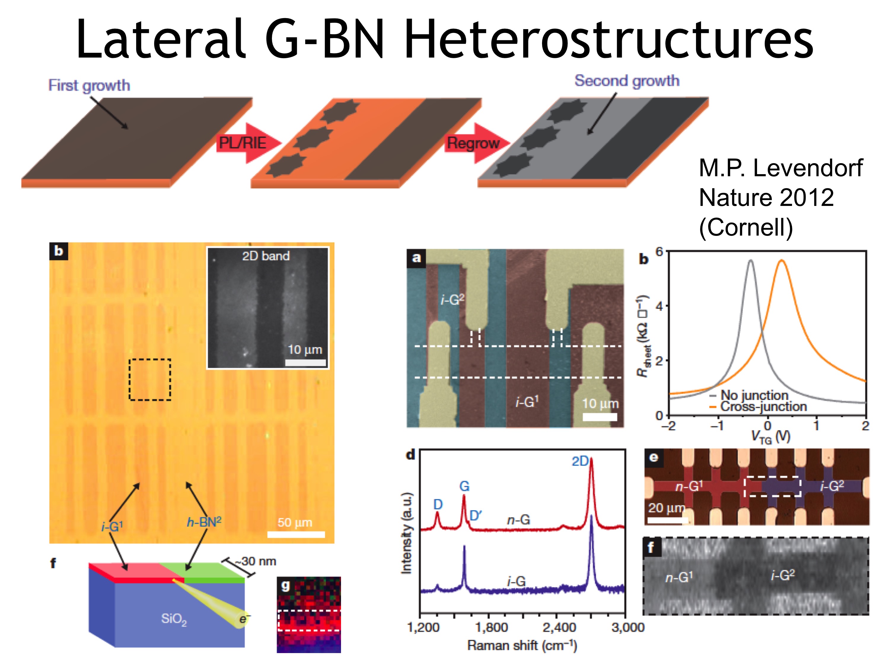
In 2012 a paper from Cornell demonstrated in experiments the possibility to pattern lateral graphene-boron nitride heterostructures, with graphene patterning and successive CVD regrowth of boron nitride. There were only limited electrical measurement in the original paper.
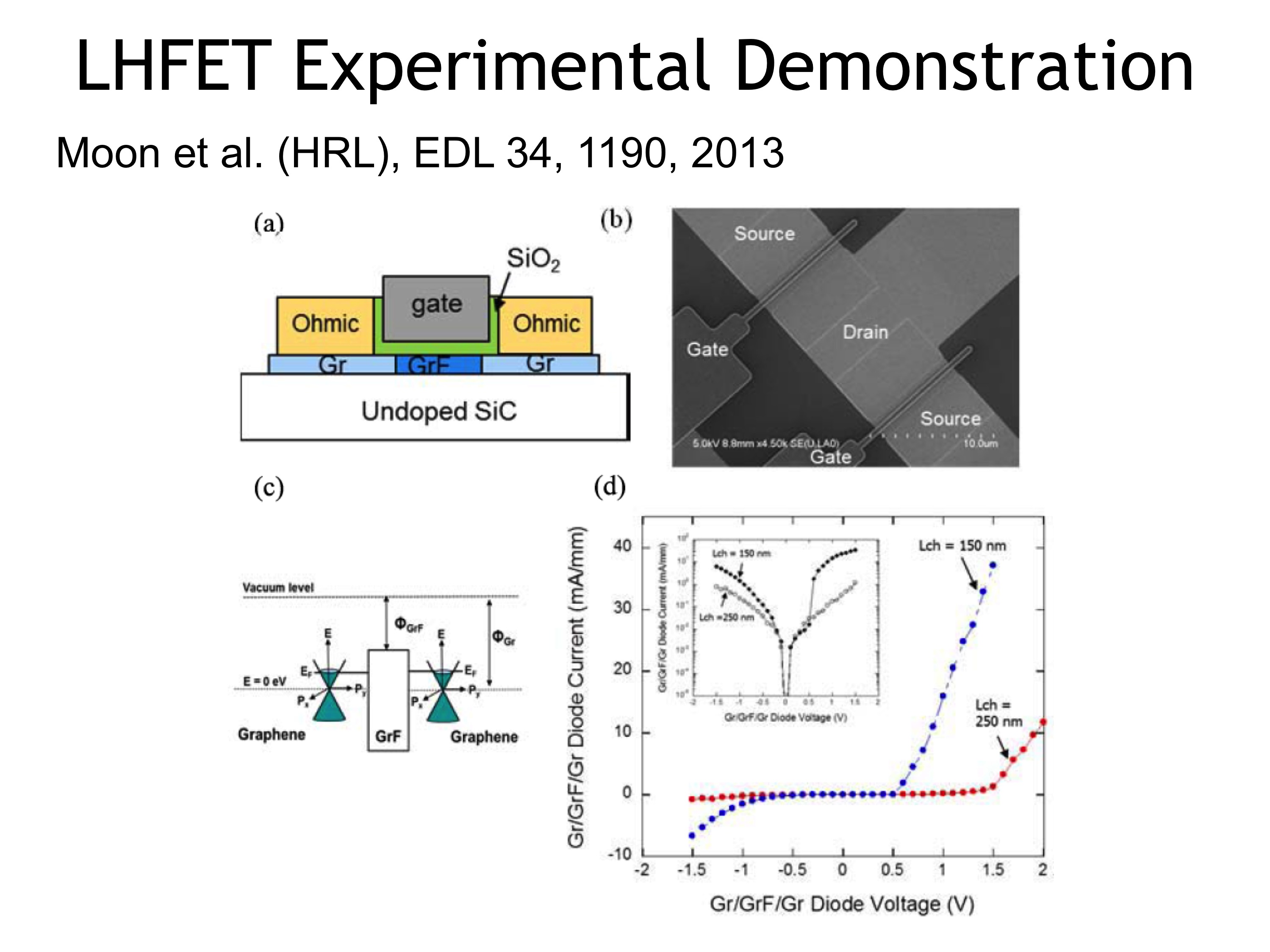
However, in 2013 this concept was demonstrated by this paper from HRL Laboratories where they used as a central region fluorinated graphene. The device works with very good Ion/Ioff ratio.
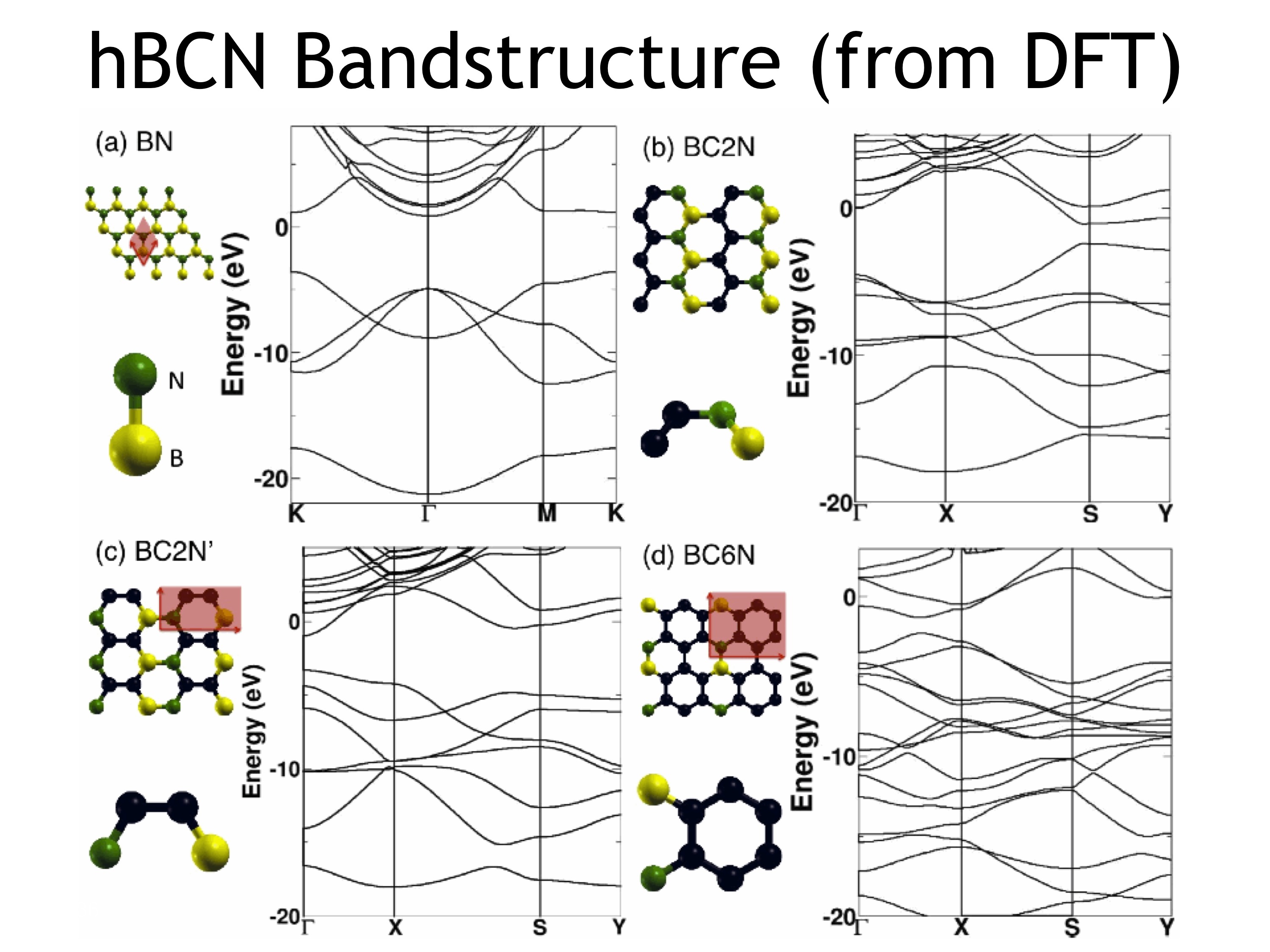
We used density-functional theory to obtain the band structure for different types of central region, and in the end we chose BC2N, which is lattice matched to graphene, and provides a valence band offsed with respect to graphene Dirac point of 0.64 eV.
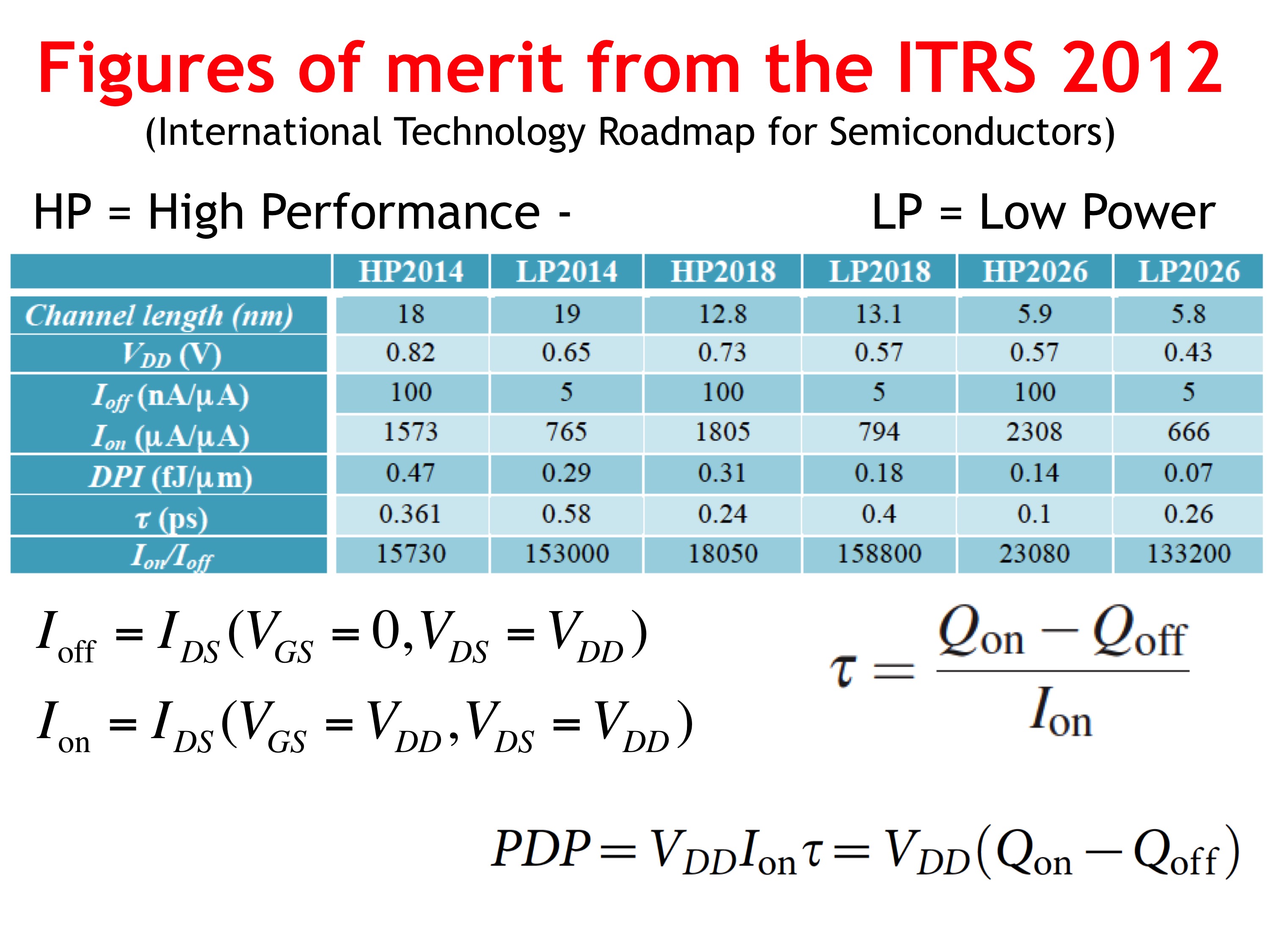
If we want to compare the potential of these devices with CMOS, we need to look at the expectations of the ITRS, 2012 edition, since it only deals with planar transistors.
Let us consider the table below, showing expectation for high performance CMOS process (HP) and for low power CMOS (LP), from 2014 to 2026.
Gate length is shrinking from 22 to 6 nm, and the supply voltage is going down to half a volt. The ratio of the “on” current (Ion) to “off” current (Ioff) is larger than 10^4.
From the point of view of dynamic performance, we have two figures of merit: the delay time, which is the ratio of the charge variation in the device between the “on” state and the “off” state, to the “on” current. And the power delay product (or dynamic power indicator), which is the product of the supply voltage, Ion and the delay time.
The delay time is a measure of speed, of computational performance. The power-delay product is a measure of energy efficiency.
As you see here CMOS are expected to remain in the fraction of ps for delay time and fraction of femtojoule per micron for the PDP.
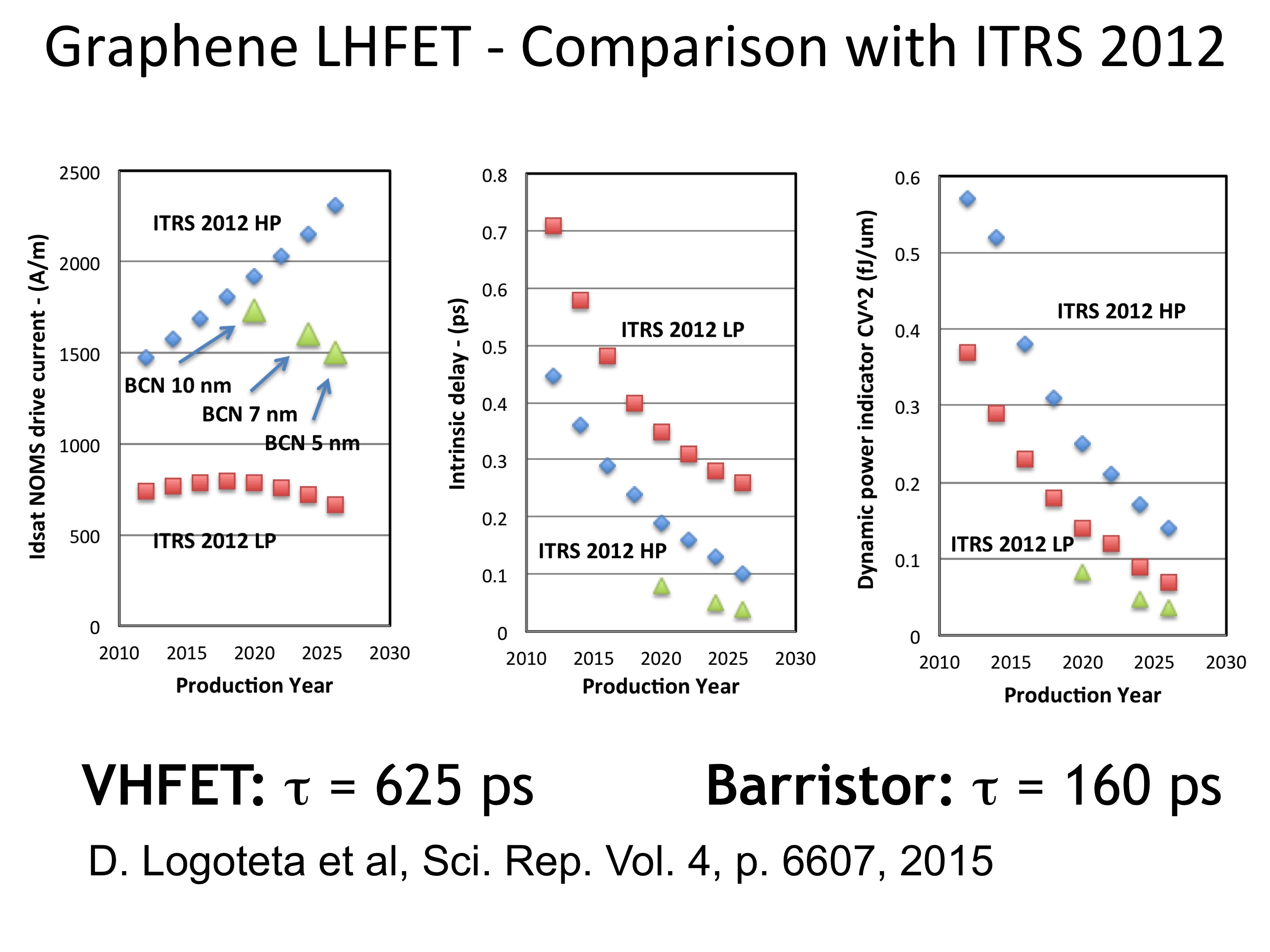
Now, we can compare at least LHFET with the ITRS2012. We chose the ITRS version because it focuses on planar transistors. The blue signs are for the high performance process, the red symbols for Low Power. We plot the On current, delay time, and power delay product as a function of the year of introduction. And we also include the BCN LHFETs with green triangles inserting them at the same year of introduction of the CMOS process with the same gate length.
You see, the delay time is better than in the case of HP CMOS, and the power-delay product is better than LP CMOS. Of course we are here considering defectless ballistic devices. But still, it is important, because the transistors based on vertical heterostructure of 2D materials, even in the most optimistic situation, provide for example a delay time that is orders of magnitude higher. More details can be found in a dedicated paper.
I am going to conclude now. The new semiconductor electronics represents a huge intellectual challenge, requiring us to address new materials, new geometries, and new physical mechanisms.
Therefore, we need to build a consistent body of knowledge drawing concepts from engineering, physics, and chemistry, and streamlining the interfaces between such disciplines. We have also to find ways to teach this new body of knowledge.
Cogliendo ogni occasione, giornali e altri media ci ricordano – neanche tanto sottilmente – che “i migliori scienziati del paese sono dovuti andare via dall’Italia”.
Ebbene, non è vero .
Poiché sono parte in causa e non voglio usare troppo spazio, mi limito a un argomento oggettivo, che chiunque può verificare.
C’è un censimento interessante compilato da VIA Academy, un’associazione di scienziati italiani all’estero: è la lista dei top italian scientists (TIS) . È una lista che non ha alcun valore ufficiale, ma si può compilare in modo quasi automatico, con dati verificabili.
La lista TIS è definita – arbitrariamente e in piena autonomia – come la lista degli scienziati di nazionalità italiana con fattore di Hirsch (h-index) maggiore di 30.
L’h-index è una misura imprecisa dell’impatto di uno scienziato – cosa veramente difficile da definire e da misurare – ma ormai è piuttosto diffusa a livello internazionale (lo trovate di chiunque su scholar.google.com). Per capirci, se un ricercatore ha un h-index uguale a 31, vuol dire che è stato autore o coautore di almeno 31 articoli ciascuno dei quali ha ricevuto almeno 31 citazioni.
Ovviamente, la lista è contestabile. Alcuni credono che l’impatto di uno scienziato non si possa quantificare. Altri che l’h-index non sia l’indice giusto (per esempio, non considera il numero di coautori di ciascun articolo). Altri ancora, che la lista usi male l’indice (per esempio usando l’h-index per definire l’impatto indipendentemente dalla disciplina e dall’età dello scienziato).
Hanno tutti ragione, ma probabilmente non abbiamo niente di meglio per ordinare liste di decine di migliaia di scienziati. E poi la lista c’è già, grazie a VIA-Academy. Quindi usiamola come riferimento, senza prenderci troppo sul serio.
Consideriamo la lista aggiornata al 10 settembre 2015: nella lista ci sono in tutto 3480 scienziati, di cui 2837 lavorano in Italia, e 75 hanno una doppia affiliazione presso un’istituzione italiana e una straniera. Anche non contando questi ultimi, più dell’80% dei top italian scientist lavorano in Italia (81.52%).
Ma allora perché si è imposta una vulgata non supportata dai fatti?
A vedere solo buonafede: per una scarsa attenzione ai numeri e un’attenzione eccessiva agli episodi e alle storie, alla “narrazione”. Oppure perché ci si concentra sui primi dieci della lista (5 dei primi 10 lavorano all’estero). Ma poiché ci sono decine di migliaia di scienziati in italia, non si coglie una tendenza basandosi su quello che fanno alcune star.
Sulla narrazione, cito sfacciatamente una cosa scritta qualche mese fa
Se lei si spiega con una narrazione non capisco più niente (direbbe oggi Flaiano)
Attenzione, non voglio dire che non ci siano problemi. Ce n’è uno in particolare enorme e molto preoccupante: L’emigrazione netta di laureati, in tutte le discipline.
Si tratta di un problema completamente diverso, legato alla struttura industriale, sociale ed economica del nostro paese. Tanto per cambiare, anche in quel caso i giornali e i politici non vogliono cogliere il punto.
Cerco di raccogliere qualche dato per un post a parte.
[1]“scienziato” si scrive con la minuscola, è un mestiere fatto da centinaia di migliaia di persone nel mondo.
Nella foto di Mario De Biasi: Enrico Fermi e Bruno Pontecorvo. Link
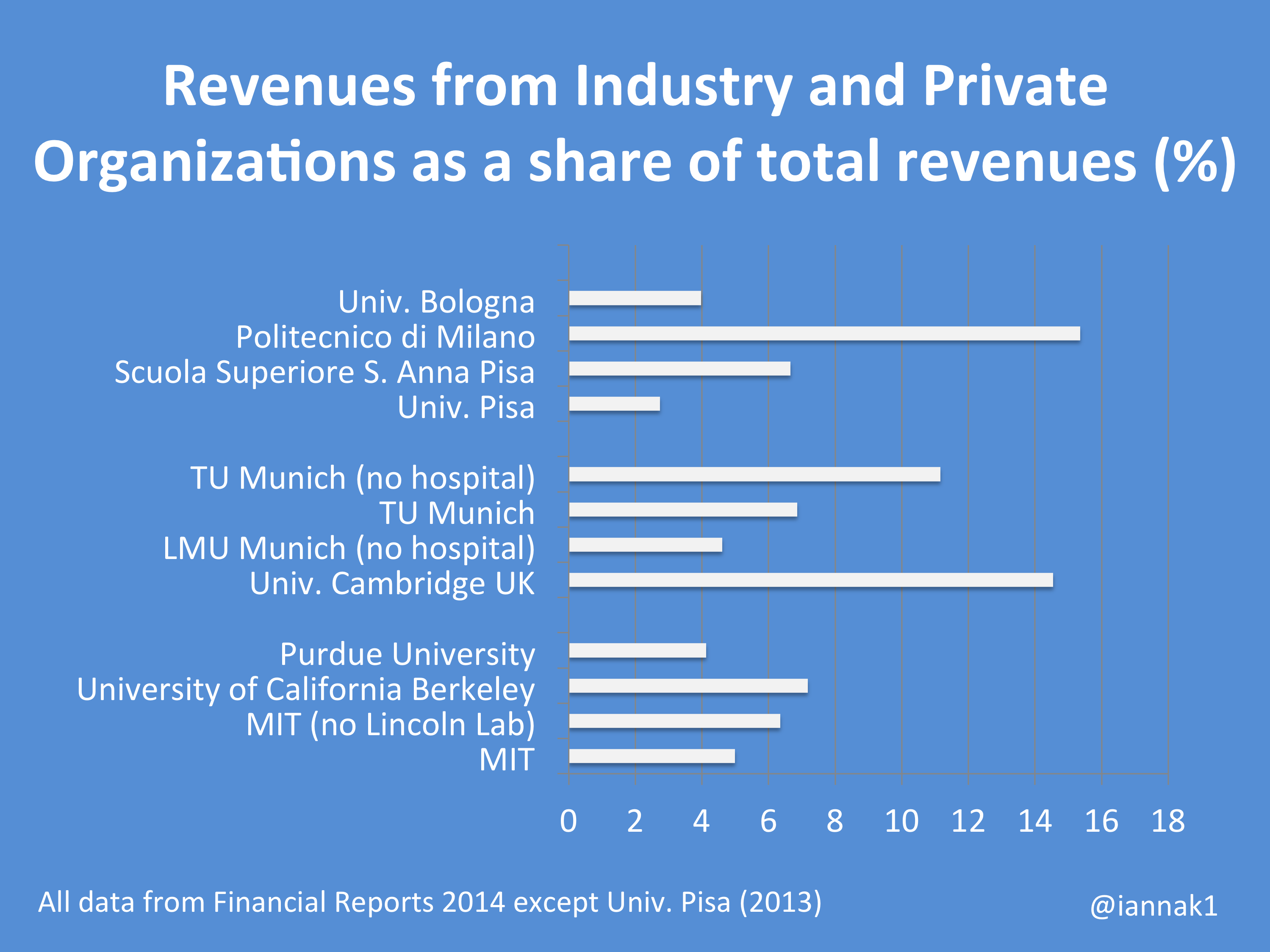
È ovvio, vero, che il Massachussets Institute of Technology (MIT) di Boston o l’Università della California a Berkeley in proporzione raccolgono molti più finanziamenti da imprese e da organizzazioni private di quanto facciano le università europee? E non parliamo poi delle italiane!
Lo sanno tutti, no?
No. È una favola.
La figura in alto mostra per alcune università americane, europee e italiane la percentuale delle entrate da industrie e organizzazioni private sul totale delle entrate. I dati sono presi dai bilanci pubblicati relativi all’anno 2014 (per l’Univ. Pisa il 2013).
Le entrate da industrie e organizzazioni private comprendono la somma delle entrate per ricerca commissionata, per servizi, per contributi alle attività di ricerca e di didattica.
Dunque, tale quota è per l’MIT il 5% delle entrate totali (194 milioni di dollari). Se togliamo dal bilancio dell’MIT le entrate del Laboratorio Lilcoln per la sicurezza nazionale, finanziato dal governo e dalle forze armate con più di 800 milioni di dollari all’anno, la quota sale al 6.3%.
Per Berkeley la percentuale è un po’ più alta: 7.2%. Berkeley è un’università generalista, ma vicina a Silicon Valley. Per una land-grant University come Purdue, in Indiana – lontano dai principali centri di innovazione industriale del paese – è il 4.1%.
In Europa la quota delle entrate provenienti da industrie e privati è simile o più alta. Come ci si può aspettare, i politecnici hanno una percentuale maggiore, per la loro affinità alle attività industriali: il Politecnico di Monaco di Baviera (TUM) è all’11.2 % (se si scorpora dal bilancio l’ospedale ) e il Politecnico di Milano è al 15.4%. L’Università di Cambridge, che non è un politecnico ma ha una particolare vocazione scientifico-tecnologica, è al 14.5%, con circa 140 milioni di sterline. Per Cambridge almeno i due terzi di questa cifra vengono dalla generose fondazioni: per esempio, 48 milioni dal Wellcome Trust, e 32 milioni da Cancer Research UK. La scuola superiore S. Anna, che è un ateneo sui generis perché non dà titoli di laurea, ha comunque una natura politecnica ed è al 6.7%.
Le altre università europee nella lista sono generaliste, e sono comunque vicine alla percentuale delle americane: Ludvig Maximilian di Monaco il 4.6% (escludendo l’ospedale), Bologna il 4%, Pisa il 2.7%.
I numeri completi sono riportati nella tabella in calce al post.
Qualche commento finale:
Raramente il finanziamento da industrie e da fondazioni private supera il 10% del totale delle entrate. Nessuna università si è svenduta ai privati, dunque. Per tutte le Università di prestigio le entrate arrivano in parte principale dallo stato, sotto forma di finanziamento ordinario o “appropriation” (solo per le università pubbliche) e di ricerche e/o servizi commissionati o attribuiti con bandi competitivi. Dai 3 miliardi di dollari di entrate dell’MIT (escluso il laboratorio Lilcoln), una fondazione privata, circa 194 milioni sono da industria e privati, e circa 324 milioni dalla tasse di iscrizione. Il resto sono fondi di ricerca pubblici in primis e poi rendite degli investimenti (“l’endowment”)
La quota di finanziamento da industrie e fondazioni in Italia è simile a quella delle università nei primi posti dei ranking internazionali. Sono i valori assoluti di tutti i finanziamenti ad essere troppo bassi. Di conseguenza, il finanziamento pubblico alla ricerca – che deve essere la quota maggiore – è particolarmente carente.
In assenza di incremento di finanziamento pubblico alla ricerca, sembra realistico puntare a finanziamenti da industrie e fondazioni intorno al 5% per un’università generalista.
L’avvicinarsi delle elezioni del nuovo Rettore è un’occasione per riflettere e discutere su come vogliamo che evolva la nostra Università. In questo spirito, le sintetiche note che seguono sono un inizio di riflessione, nella consapevolezza che ciascun punto richiederebbe un trattamento più approfondito e una discussione separata.
È vero che le decisioni e le relative attuazioni dipendono da molti fattori esterni e dal consenso nei processi democratici interni. Non di meno, è importante che ci sia una visione chiara, condivisa e realistica della direzione in cui condurre l’Università, in modo da comporre in modo coerente le forze interne e le occasioni propizie provenienti dall’esterno. Credo che il nuovo Rettore debba essere eletto per la nostra fiducia nella sua visione e nel suo impegno a realizzarla.
A mio parere, una nuova visione per l’Università di Pisa deve tenere conto di alcuni dati di fatto che si sono manifestati con chiarezza negli ultimi anni:
A livello nazionale, non è realistico che ci sia un aumento cospicuo delle risorse destinate al sistema universitario, data la situazione della finanza pubblica.
A livello internazionale, il sistema universitario sta diventando sempre più globale. La mobilità degli studenti e dei lavoratori della conoscenza è aumentata, i percorsi educativi in nazioni diverse sono ormai confrontabili. L’attenzione della politica e dell’opinione pubblica in tutti i paesi alle classifiche internazionali delle università è un effetto di questo processo.
Il prestigio di un Ateneo non si basa più solo sulla formazione della classe dirigente (un tempo), o sulla formazione dei lavoratori della conoscenza (più recentemente), ma sempre più sull’impatto dell’Università sulla vita sociale, economica e culturale della nazione. Il prestigio è prezioso, perché favorisce l’acquisizione di risorse da finanziatori pubblici e privati, con cui accrescere ancora impatto e prestigio. Su questo ciclo virtuoso si basa la forza delle migliori università del mondo.
In questo contesto, credo che sia fondamentale che il nostro Ateneo punti con decisione al modello delle grandi Università di Ricerca[1].
Il motivo è semplice: solo le grandi università di ricerca riusciranno in un sistema universitario globale a mantenere identità riconoscibile e prestigio, e quindi ad acquisire le adeguate risorse economiche e umane. È l’unico modo di innescare il ciclo virtuoso che consente agli studenti di ottenere un’educazione migliore e un titolo più apprezzato, ai ricercatori e agli studiosi di svolgere un lavoro migliore, al paese di crescere culturalmente, economicamente, socialmente. L’alternativa è pericolosa, perché per lo stesso meccanismo, una iniziale perdita di prestigio può portare a un’accelerazione verso il basso.
Con quali risorse? L’aspetto su cui possiamo realisticamente agire è l’acquisizione di risorse proprie, in termini di ricerche commissionate, ricerche con finanziamenti competitivi e offerta didattica complementare.
Le nostre risorse proprie sono molto minori di quelle delle acclarate grandi università di ricerca. Per esempio, l’Università di Pisa e l’Università di Cambridge sono confrontabili per numero di docenti, per numero di laureati, e per finanziamento pubblico di base (246.2 milioni di euro per Pisa, 178.6 milioni di sterline per Cambridge)[2]. L’Università di Pisa ha raccolto nel 2013 circa 27.5 milioni di euro dalla ricerca, mentre l’università di Cambridge 371.8 milioni di sterline. È vero che il Research Council e le fondazioni del Regno Unito (soprattutto la Royal Society) sono molto più generose del nostro ministero in termini di finanziamenti alla ricerca, e che Pisa ha molti più studenti. Però, anche solo considerando i programmi quadro della Commissione Europea, l’Università di Cambridge ha raccolto più di 6 volte i finanziamenti raccolti dall’Università di Pisa.
È necessario incrementare notevolmente gli importi raccolti con le ricerche commissionate e le ricerche con finanziamenti competitivi. Una serie di misure concertate potrebbero renderla una priorità dell’Ateneo:
Forte supporto centralizzato ai dipartimenti, ai docenti, e al personale amministrativo;
Coordinamento di azioni collettive e creazione di strutture ad hoc per poter accedere ai grandi finanziamenti e stabilire accordi strategici con grandi organizzazioni, non accessibili ai singoli gruppi di ricerca.
Allineamento degli incentivi per le strutture e per i singoli a questo obiettivo, in modo da liberare le energie e le eccellenze di cui l’Università già dispone, focalizzarle sullo sviluppo dell’Ateneo, e permettere loro di lavorare al meglio.
Coordinamento centralizzato di iniziative di raccolta fondi per lo svolgimento di ricerche di interesse pubblico.
Credo che sia realistico l’obiettivo di raddoppiare il totale dei fondi raccolti per la ricerca in cinque anni.
Le classifiche internazionali sono parziali, incomplete e a volte deformi. Ma sono l’effetto di un sistema effettivamente globalizzato in cui il singolo può decidere dove studiare per la laurea triennale, dove studiare per la laurea magistrale, e la singola organizzazione può decidere con quale ateneo stabilire un rapporto privilegiato. Essere in alto in tali classifiche ha una forte correlazione con l’essere rinomati su scala globale, per ricerca e per prestigio.
Reperire maggiori risorse e allineare gli incentivi può consentire di incrementare l’impatto in qualità e quantità della ricerca dell’Ateneo.
Un altro aspetto fondamentale, nell’era dell’informazione, è il prestigio dell’Università nella comunità universitaria e nell’opinione pubblica. Aumentare il prestigio richiede una moltiplicazione degli sforzi di comunicazione interna ed esterna, la promozione continua dei migliori risultati raggiunti da tutti i membri della comunità, l’impegno in attività di divulgazione tra il pubbico (outreach), e in altre attività che abbiano impatto sulla vita culturale e sociale della nazione. Tra esse ci sono senz’altro le attività che costituiscono la cosiddetta terza missione, in cui la nostra università è cresciuta molto negli ultimi anni e in cui ancora c’è ancora molto spazio per crescere. La terza missione può rendere il nostro Ateneo il motore principale della cultura e dell’innovazione industriale nella nostra regione e uno dei maggiori del paese.
Non è semplicemente accettabile che piccole realtà appaiano confrontabili o addirittura migliori del nostro Ateneo agli occhi dell’opinione pubblica. Se tutta la comunità universitaria fosse chiamata a partecipare a questo impegno, si potrebbe accrescere o in alcuni riscoprire l’orgoglio di far parte di questa Università.
La didattica trarrebbe forti vantaggi dall’impegno sul fronte della ricerca e del prestigio. Considerare didattica e ricerca come priorità alternative non ha riscontro nella realtà: per esempio, la classifica internazionale degli atenei del Times Higher Education per la didattica è fortemente correlata con quella per la ricerca. Perché, nel tempo, risorse e prestigio consentono di attirare e supportare gli studenti, docenti e non docenti più motivati.
L’aumentata mobilità degli studenti fa sì che siano sempre più frequenti i casi che laureati di un ateneo decidano di conseguire la laurea magistrale in un’altra università. È quindi importante trattare e promuovere i corsi di laurea magistrale come percorsi educativi autonomi, farli conoscere e proporli alla più ampia platea possibile di studenti, renderli uno dei principali fattori di attrazione per l’Università.
I corsi di laurea e laurea magistrale del nostro ateneo sono più di 100. È fondamentale sperimentare innovazioni su alcuni corsi di laurea. Per esempio, è utile proseguire con l’offerta degli insegnamenti in inglese, è utile sperimentare i corsi in collaborazione con altri atenei e fuori Pisa, i corsi a distanza, le summer school, la cosiddetta educazione continua, i master. Nello spirito della sperimentazione, sarà veramente importante stabilire dei criteri di successo e monitorare ogni esperimento, per estendere prontamente ciò che funziona e interrompere ciò che non funziona.
Alcune forme di didattica innovativa, quali master e corsi di educazione continua per chi già lavora o ha lavorato, rappresentano una risposta diretta dell’università alle esigenze del mondo del lavoro e sono un’opportunità importante sia per migliorare l’impatto dell’università sulla società, sia per incrementare le risorse proprie. Anche in questo caso, è fondamentale riallineare gli incentivi dei singoli e delle strutture agli interessi dell’Ateneo e del territorio.
È fondamentale per i nostri studenti potenziare ancora le attività di job placement per tutti i titoli di studio, incluso il dottorato, e attivare iniziative per seguire gli studenti dopo gli studi e negli anni del lavoro, coltivare negli anni il legame tra ex-alunni e università, fare dell’orgoglio dei nostri ex-alunni la migliore testimonianza del nostro lavoro. Inoltre, è necessario usare queste attività per raccogliere nuovi elementi di conoscenza che informino la progettazione e l’evoluzione dell’offerta didattica.
Infine credo sia fondamentale per il nuovo governo dell’Ateneo curare lo sviluppo del personale docente e non docente, attraverso un piano di sviluppo condiviso e un assetto organizzativo che valorizzi le capacità e le prerogative di ciascuno.
Le sfide che l’Università di Pisa dovrà affrontare nel nuovo scenario internazionale saranno ardue e complesse: è necessario che ciascuno di noi usi al meglio le proprie capacità facendo ciò che sa fare meglio.
È importante che il personale docente si possa concentrare sulla didattica e sulla ricerca, nello svolgimento delle attività quotidiane e nella progettazione e guida della didattica e della ricerca. È importante che il personale amministrativo e tecnico si possa concentrare sul funzionamento della macchina amministrativa e tecnica con adeguata autonomia esecutiva. Sembrano cose ovvie, ma spesso vediamo colleghi docenti esasperati per le numerose pratiche burocratiche e amministrative di cui si devono fare carico, e colleghi non docenti altrettanto esasperati per l’affidamento di responsabilità amministrative e organizzative a docenti poco interessati e inclini al ruolo.
Il miglioramento dell’assetto organizzativo richiede da un lato un ulteriore deciso snellimento delle procedure e dei regolamenti, e dall’altro una chiara ed efficiente attribuzione dei ruoli e dei compiti, sia tra dipartimenti e amministrazione centrale, sia tra docenti e non docenti. Il prestigio e la credibilità dell’Università come motore dell’innovazione in Italia richiede anche che l’Università sia un modello per assetto organizzativo e per efficienza delle procedure organizzative e operative, sfruttando pienamente l’autonomia di cui gode.
Lo sviluppo del personale è soggetto ai repentini cambiamenti di linea del legislatore. Per questo motivo è importante avere priorità chiare, in modo da utilizzare in modo coerente – con un piano condiviso – le occasioni di azione concesse dal legislatore e dal governo nazionale.
È importante allineare le priorità di sviluppo del personale al modello di università che vogliamo, superando l’ancoraggio prevalente al fabbisogno didattico, che si addice più a una teaching university. Per essere stabilmente tra le grandi università del mondo, dobbiamo avere priorità adeguate, allineare gli incentivi dei singoli al nostro modello di Università, procedere di conseguenza allo sviluppo del personale.
L’ultimo punto è dedicato a chi non voterà per il futuro Rettore. L’età media di ingresso nei ruoli è troppo alta, per responsabilità soprattutto del legislatore. Il problema è drammatico, perché è raro il personale di ruolo con meno di quaranta anni. Sarà importante che il nuovo Rettore porti l’Ateneo a una soluzione condivisa, che attenui la vacanza generazionale che si è creata.
Come avevo anticipato, si tratta di note sintetiche e incomplete, di un inizio di riflessione su aspetti che discutiamo raramente, presi come siamo dallo svolgimento del lavoro quotidiano. Ma tra meno di un anno si voterà per un nuovo mandato rettorale, ed è il momento alzare lo sguardo verso il futuro.
[1] Nella classificazione Carnegie, l’università di Pisa è già una VH/RU (Research University with Very High research Activity). Delle 4000 istituzioni universitarie americane, 108 sono classificate VH/RU. In questo contesto, per grande università di ricerca intendo una delle migliori VH/RU.


