New Student Projects 2015 – Progetti per Tesi e Internship

Nuova lista aggiornata a febbraio 2015 con argomenti per progetti di tesi o internship. Ci sono sia tesi in Italia, sia all’estero. Per le tesi all’estero, il mio vincolo è che deve essere un progetto su un tema su cui abbiamo un’attività di ricerca, in modo da seguire a distanza e incidere in modo significativo sul lavoro. Adesso è in una pagina dedicata, e sarà aggiornata con continuità.

New list of student projects updated to February 2015. Now is in a dedicated page, and will be updated continuously. Projects title are in English, descriptions in Italian (for international students, just contact me for details).

Share this:

Presentation: Graphene and 2D electronics

I gave this presentation on Graphene and 2D Electronics at the Marie-Curie Conference 2013 in Florence, on Nov. 25. It was an session with mindblowing presentations especially from renown surgeon Ugo Boggi and CMS emeritus spokesperson Guido Tonelli. As I knew, speaking just after a superstar physicist is really really challenging.

Everybody had to keep their presentations understandable by a general audience of researchers and Marie-Curie fellows from diverse disciplines: hard sciences, social sciences, and humanities. And to stay within 12 minutes. For this reason I think this presentation can be enjoyable by casual visitors of my website. Enjoy.

However, the whole session was humbling. I was really honoured and thankful to the organizing committee for the invitation. Most of all, it was great fun.

(illustration by Argonne National Lab)

Share this:

Grafene ed elettronica ultra sottile – 9 minuti di video

Il 20 settembre ho partecipato a una giornata di presentazione delle attività nel campo della Knowledge Acceleration & ICT presso la nostra Università.

Ho parlato per nove minuti nove delle nostre attività sull’elettronica in grafene, calibrando il discorso per un pubblico non necessariamente esperto dell’argomento.
Ne è uscita una presentazione veloce, semplice e in italiano, su uno dei temi che ci ha tenuto più impegnati, negli ultimi sei anni. E su cui stiamo lavorando molto.

Il video è qua sotto (Bella tendenza i video online di ogni evento, e bella idea quella di seguire la tendenza bene e presto).

Mi è tanto comodo questo video, per dare il puntatore a chi spesso chiede: ma che è sto grafene? che ci fate?

Cliccando sulla playlist si vedono anche le altre presentazioni della giornata.

Share this:

Talk on Graphene transistors and two dimensional electronics

Last week in Berlin for INC9 I gave a talk on “Graphene transistors and two dimensional electronics”, sharing our views on the future of graphene electronics. The presentation is below.

[slideshare id=21459933&doc=iannacconeinc9polished-130519124601-phpapp01]

Most of the activity has been funded from the European Commission in a series of projects. We still have many ideas and many possibilities for student work, graduate and postgraduate work on the topic.

Share this:

Originality in Research can work against Science

I’ve encountered some situations in recent weeks that made me think about a short essay in Hackers and Painters by Paul Graham: “Design and Research“. In particular, this paragraph:

The difference between design and research seems to be a question of new versus good. Design doesn’t have to be new, but it has to be good. Research doesn’t have to be good, but it has to be new. I think these two paths converge at the top: the best design surpasses its predecessors by using new ideas, and the best research solves problems that are not only new, but actually worth solving. So ultimately we’re aiming for the same destination, just approaching it from different directions.


Using old ideas in new ways that actually work better, is actually considered less interesting in research than  proposing original ideas that have have such apparent drawbacks that make them totally useless (if you do not count writing a paper as “use”).

This issue is of course very serious in engineering and all the so-called “applied sciences”. In those fields, when you propose something new, you typically have an incumbent technology or technique to use as a benchmark.

But it is serious in an even subtler way in the so-called “basic sciences” [1]. Indeed, since several years, as a way to increase the chance of getting funded in basic science projects, researchers are repackaging them as “applied science” projects, or simply stress the fact that results can have a large impact on applications. Examples of the latter are “mesoscopic transport”, “quantum computing”, or “molecular electronics”, just to name few fields I’ve been working on or close to. What I observe repeatedly is the proposal of new ideas, new devices, revolutionary technology without a due diligence, a detailed understanding on the incumbent solutions and of the important metrics for that field of application.

There is also another issue in which originality in research works against science. For science to work, experiments should be tested and reproduced several times. However, all credits goes to the first. If you are just the second, your work gets published in a less exclusive journal. Therefore if often happens that competitive research groups in a rush to complete an experiment just stop – if another group finish first and publishes results – and start working on something else. This is bad for science, because experimental results are less verified than they should be. This happens also for complex theoretical derivations and numerical simulations, because you typically cannot even publish as a second, unless you find an error in the first work.

One should not be surprised, by this behavior, anyway. Scientists are simply professionals, and of course they respond to professional incentives.

This is also true for me. I appreciate the multifaceted advantages of originality, and have choses to focus on new device or circuit concepts and on new methodologies. However, I have in time published several papers on the tune of “why this proposed technology cannot work”. I will continue, since I believe it is important. Still, it makes you appear as a grumpy old man.

[1] At my venerable age, I have not really understood the difference between basic science, applied science, and engineering, for that matter. That is why I use to specify “so-called”. but this will be the topic of another post.

Related posts:

Share this:

The economic status of higher education

An extremely interesting blog post by Marc Cuban on the economic status of higher education in the US. I really enjoy Marc Cuban’s posts, since he always goes straight to the issue. I think he has a couple of good points, that resonate with some of my thoughts:

  1. We have always considered a good thing to have a higher percentage of graduates, as in the US, UK, France, Germany. In 2010 the percentage of graduates in Italy was 13%, compared with 30% in the US and 24.2 in EC12). Not all degrees can lead to a well-paid job. I covered in part this issue here (post in Italian). Now we probably should reflect on the fact that some countries might have overshot. And it does not depend on whether the University system is public, mostly public, or mostly private. It is a call to reconsider the relevance of technical and vocational high schools.
  2. Higher education as an economic activity has not followed the deflationary path or the productivity improvements that other economic activities have experienced, pushed by globalization and ICT technologies [1][2]. In the US they have actually gone the opposite direction in recent years, with a large increase in academic fees fueled by student debt. I think at this point the “classical” model of the research University is at risk, unless an updated scalable model can be found. I covered some of the points here (in Italian), but plan to talk about it some more in one of the next posts. For those interested, there’s a great recent opinion piece on this issue by David Brooks on the NYTimes.

[1] This is also true for the national health systems both in Europe and in the US.

[2] Oh yes: higher education is an economic activity. I do not mean it is “only” an economic activity.

Share this:

New NanoTCAD-ViDES Released!

This week we have released the new version of NanoTCAD-ViDES.

NanoTCAD ViDES it is a software package for the simulation of nanoscale electron devices and materials on an atomistic basis, using non-equilibrium Green’s functions formalism for the solution of the Schroedinger equation with open boundary conditions, and full three-dimensional electrostatics.

It is a major new release! My colleague and lead developer Gianluca Fiori put in incredible energy to make available to the computational electronics community a versatile and powerful simulation tool. Yes, because NanoTCAD-ViDES is released as open source with BSD license.

We have also launched a dedicated website: vides.nanotcad.com, where one can find the source code and full documentation, lots of detailed tutorials, how to work with us to improve the code, a list of papers based on ViDES.

This release of NanoTCAD ViDES  is a python module, so that we can leverage the whole flexibility of the most science-friendly scripting language. The new structure is extremely modular and makes it very easy to add new modules for additional materials, functionality, and physics.

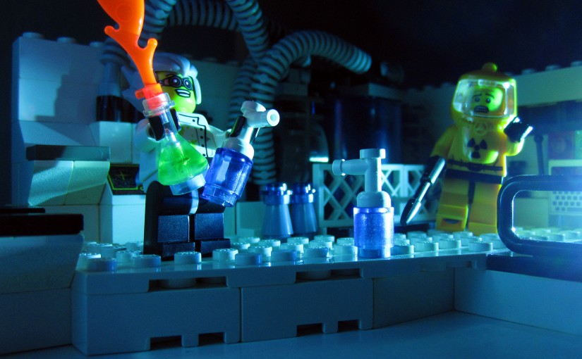
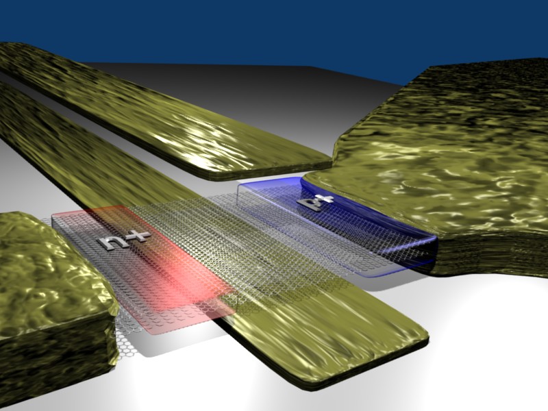
As of now, we have released the code with a set of predefined functions, to compute transport in graphene nanoribbons, carbon nanotubes, two-dimensional mono-layer and bilayer graphene transistors. Basically it is  the set of devices and structures for which we have used the code up to now. Most of them are illustrated in the beautiful figures above.

We wil be adding new modules as we develop them and use them in our research.

A module for zincblend crystals, such as silicon, germanium, and III-V, is coming soon, based on a sp3d5s* tight-binding Hamiltonian. In the next future also modules for hexagonal boron-carbon-nitride compounds will be released.

As you can see, I am really enthusiastic of this new development, and I really can’t wait to see how ViDES continues and grows.

We started the adventure in nanoelectronics TCAD several years ago with the NanoTCAD project, funded by the European Commission in 1999, which really meant a lot to me and to my career as a scientist (a non-expert news article here). After few almost complete rewritings, thanks to Gianluca’s technical leadership, the code is ready for a new phase, with a much larger base of users and contributors.

With Gianluca, I’d love to thank also the other scientists that have contributed to the code: Alessandro Betti, Paolo Marconcini, and Pino D’Amico. I hope this list becomes very long.

If you are a scientist working on computational nanoelectronics, just consider the opportunity. You can leverage the great capabilities of NanoTCAD ViDES by contributing to the code. You can focus your effort only on the new module that is of interest to you, and use the perfectly validated and tested 3D electrostatics and NEGF module. I would call this maximum leverage. The BSD license ensures you full ownership of what you write. If you think you can take advantage of collaborating with us on this, just drop us a line. We have wonderful experiences of remote and very fruitful collaboration: the Internet works!

As a finishing word, if you want to work with us in Pisa on computational nanoelectronics and on extending NanoTCAD ViDES, contact me. If you have a strong background on device electronics or condensed matter physics, and really know how to program (this link if you understand Italian), we can have positions available in Pisa, from few months to few years. Even if you are a MS student looking for a thesis subject or a summer job, just drop me a line. But be prepared for a tough interview!

P.S.

If you are interested, signup here to our newsletter dedicated to NanoTCAD ViDES, with release updates and news on research results.

Share this:

Il materiale delle meraviglie

TFET

Giuseppe Iannaccone

pubblicato su Il Tirreno, 6 ottobre 2010

Ieri, per un attimo, abbiamo avuto la sensazione di essere tornati agli albori del premio Nobel. Nei primi anni del ‘900 venivano premiati scienziati giovani, pochi anni dopo la loro scoperta rivoluzionaria. Così fu per Pierre e Marie Curie, per Einstein, per Marconi. Nel tempo, questa tradizione si è persa, e abbiamo cominciato a vedere scienziati ormai in pensione ricevere il premio per un contributo alla scienza dato in gioventù.

E invece ieri André Geim e Kostantin Novoselov, dell’Università  di Manchester, hanno ricevuto il premio Nobel per la Fisica per una scoperta del 2004. Solo sei anni fa sono riusciti a manipolare della comune grafite per ottenere uno strato di Grafene, un materiale cristallino costituito da uno strato di carbonio dello spessore di un singolo solo atomo. Il grafene è diventato subito “the wonder material”, il materiale delle meraviglie. E’ il materiale conosciuto più resistente alla trazione; il miglior conduttore elettrico a temperatura ambiente; è flessibile e praticamente trasparente. E poi, è bello. Gli atomi di carbonio si dispongono in una struttura planare ad alveare, con leggere ondulazioni, e tanto basta perché la materia acquisti proprietà  fisiche nuove, spesso impreviste, e dotate di quella bellezza che muove gli scienziati.

Dal 2004, è partita una vera caccia all’oro su scala globale. Fisici, Chimici ed Ingegneri nei laboratori di ricerca di tutto il mondo sono stati attratti dal nuovo materiale. Sono riusciti a realizzare fogli di grafene in modo sempre più efficace e privo di difetti, e a rivelarne in modo più completo le proprietà  fisiche e chimiche.

Scienziati più orientati a sfruttarne le proprietà  in applicazioni stanno valutando le potenzialità del materiale per la realizzazione di sistemi elettronici e fotonici – per il calcolo e la comunicazione – e di sensori nel campo delle tecnologie biomediche. Per esempio, presso l’Università  di Pisa, noi ingegneri stiamo cercando di capire se il materiale delle meraviglie può essere usato per realizzare transistori veloci. Bravissimi colleghi fisici della Scuola Normale e dell’Università  di Pisa, sono concentrati sullo studio delle proprietà  fisiche di base del materiale.

La prima scoperta pionieristica di Geim e Novoselov è stata seguita da decine di migliaia di lavori scientifici in pochissimi anni, realizzati da migliaia di scienziati. Un tale impatto meritava un Nobel, era solo questione di tempo. La tempestività, stavolta, ha stupito positivamente.

E’ ancora presto per dire se e come il grafene cambierà  la nostra vita. Spesso le applicazioni rivoluzionarie non sono prevedibili fin dall’inizio. Ma le proprietà  del materiale sono così belle che siamo in molti a scommettere non rimarranno inutilizzate. Il grafene è un bambino di sei anni. Ha tutta la vita davanti.

[Image: Copyright IEEE, Gianluca Fiori]

Share this: